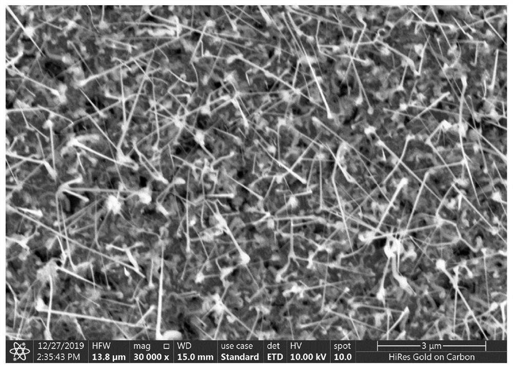
Preparation method of germanium and tin nano material under normal pressure
A nano-material, germanium-tin technology, applied in the field of preparation of germanium-tin nanomaterials under normal pressure, can solve the problems of difficult removal of reagents, harsh temperature and pressure conditions, expensive equipment, etc., and achieve the effect of easy operation and simple equipment
- Summary
- Abstract
- Description
- Claims
- Application Information
AI Technical Summary
Problems solved by technology
Method used
Image
Examples
Embodiment 1
[0029] A kind of preparation method of germanium tin nanometer material under normal pressure, utilize see figure 1 The experimental apparatus shown was prepared, including the following steps:
[0030] Select a silicon wafer with a length and width of 10mm*10mm for cleaning: first, ultrasonically clean it with acetone solution for 20 minutes to remove organic matter on the surface of the silicon wafer, and then rinse it with deionized water;
[0031] Platinum spraying: 4nm thick platinum is sprayed on the dry silicon wafer surface;
[0032] Place the silicon wafer sprayed with platinum on one end of the tube furnace, with the side sprayed with platinum facing up;
[0033] Place 0.5g of germanium powder and 0.025g of tin powder at the other end of the tube furnace, and continuously feed inert gas into this end, then raise the temperature of the tube furnace from room temperature to 850°C at a rate of 5°C / min, and keep it warm. After 60 minutes, the temperature was lowered to...
Embodiment 2
[0035] A kind of preparation method of germanium tin nanometer material under normal pressure, utilize see figure 1 The experimental apparatus shown was prepared, including the following steps:
[0036] Select a silicon wafer with a length and width of 10mm*10mm for cleaning: first, ultrasonically clean it with acetone solution for 20 minutes to remove organic matter on the surface of the silicon wafer, and then rinse it with deionized water;
[0037] Bismuth spraying: 4nm thick bismuth is sprayed on the dry silicon wafer surface;
[0038] Place the silicon wafer sprayed with bismuth on one end of the round-bottomed porcelain boat, with the side sprayed with bismuth facing up;
[0039] Put 0.25g of germanium powder and 0.025g of tin powder on the other end of the round-bottomed ceramic boat, then place the round-bottomed porcelain boat in the tube furnace, and place the end containing the germanium powder and tin powder in the tube furnace At the same time, after continuousl...
Embodiment 3
[0041] A kind of preparation method of germanium tin nanometer material under normal pressure, utilize see figure 1 The experimental apparatus shown was prepared, including the following steps:
[0042] Select a silicon wafer with a length and width of 10mm*10mm for cleaning: first, ultrasonically clean it with acetone solution for 20 minutes to remove organic matter on the surface of the silicon wafer, and then rinse it with deionized water;
[0043] Nickel spraying: 4nm thick nickel is sprayed on the dry silicon wafer surface;
[0044] Place the silicon wafer sprayed with nickel on one end of the round-bottomed porcelain boat, with the side sprayed with nickel facing up;
[0045]Put 0.5g of germanium powder and 0.025g of tin powder on the other end of the round-bottomed ceramic boat, then place the round-bottomed porcelain boat in the tube furnace, and place the end containing the germanium powder and tin powder in the tube furnace At the same time, after the inert gas is ...
PUM
 Abstract
Description
Claims
Application Information
 - R&D Engineer
- R&D Manager
- IP Professional
- Industry Leading Data Capabilities
- Powerful AI technology
- Patent DNA Extraction
Browse by: Latest US Patents, China's latest patents, Technical Efficacy Thesaurus, Application Domain, Technology Topic, Popular Technical Reports.
© 2024 PatSnap. All rights reserved.Legal|Privacy policy|Modern Slavery Act Transparency Statement|Sitemap|About US| Contact US: help@patsnap.com


