


Quick Research
Generate reliable direction feasibility study reports for your R&D in just a few steps.

Technical Q&A
Discover and master advanced knowledge NOW. Basics, ideas, possibilities, all at once.

Find Solutions
As an expert in R&D theories, this can generate solutions to your technical problems instantly.

Evaluate Feasibility
Analyze your overall solution with one click, know your potential R&D risks in advance.

Monitor Landscape
Get weekly tech updates, stay abreast of the latest tech innovations and key insights.
Heterogeneous semiconductor film and preparation method thereof
A semiconductor and thin film technology, applied in the field of heterogeneous semiconductor thin film and its preparation, can solve the problems of thermal mismatch, high preparation cost, and low utilization rate of stripped ions
- Summary
- Abstract
- Description
- Claims
- Application Information
AI Technical Summary
Problems solved by technology
Method used
Image

Examples
preparation example Construction
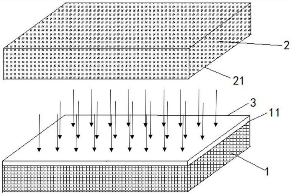
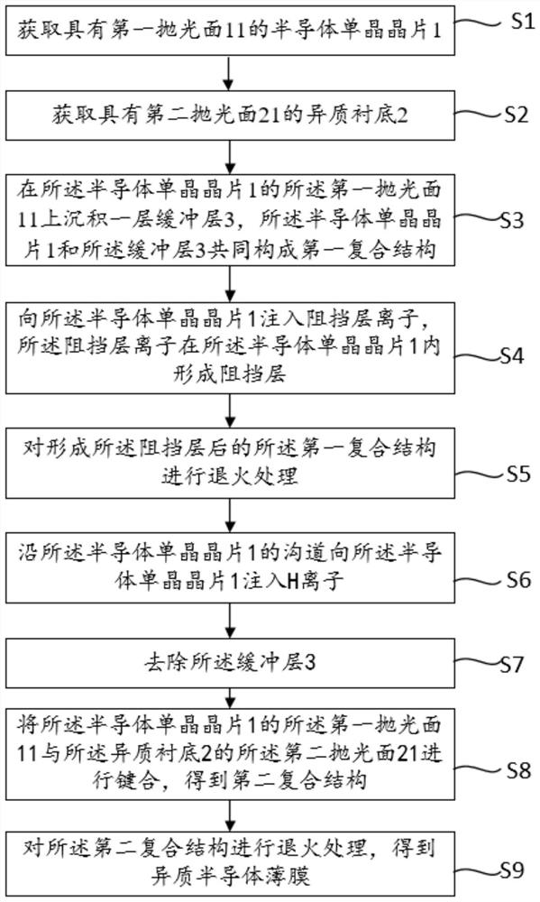
[0022] combine figure 1 and figure 2 As shown, the implementation of the present invention provides a method for preparing a heterogeneous semiconductor thin film, the method comprising the following steps:
[0023] S1. Obtain a semiconductor single crystal wafer 1 having a first polished surface 11;
[0024] S2. Acquire a second polishing surface 21 ( figure 1 heterogeneous substrate 2 where the mid-bottom surface is not visible);
[0025] S3. Deposit a layer of buffer layer 3 on the first polished surface 11 of the semiconductor single crystal wafer 1, the semiconductor single crystal wafer 1 and the buffer layer 3 together form a first composite structure;
[0026] S4, implanting barrier layer ions into the semiconductor single crystal wafer 1, and the barrier layer ions form a barrier layer in the semiconductor single crystal wafer 1;
[0027] S5. Perform annealing treatment on the first composite structure after forming the barrier layer: the annealing temperature is...
specific Embodiment approach 1
[0043] combined with figure 2 , the steps are as follows: obtain a lithium niobate single crystal wafer with the first polished surface, the size of the lithium niobate single crystal wafer is 4inch (inch), and the thickness is 500 μm (micrometer), and the surface roughness of the first polished surface is 0.5nm (nano); obtain a SiC substrate with a second polished surface, the size of the SiC substrate is 4inch, the thickness is 400 μm, and the surface roughness of the second polished surface is 0.3nm; in the first polishing of lithium niobate single crystal wafer Al on the surface is deposited with a thickness of 20nm by ALD (atomic layer deposition) 2 o 3 layer, LiNbO3 single crystal wafer and Al 2 o 3 The layers together form a first composite structure. Subsequently, the implantation energy to the lithium niobate single crystal wafer was 140Kev, and the implantation dose was 5*10 14 ions / cm 2 Ar ions, the implantation depth is 50nm from the outer surface of the buf...
specific Embodiment approach 2
[0045] combined with figure 2 , the steps are as follows: obtain a gallium nitride single crystal wafer with a first polished surface, the size of the gallium nitride single crystal wafer is 5 inches, the thickness is 460 μm, and the surface roughness of the first polished surface is 0.6 nm; obtain a gallium nitride single crystal wafer with a second polished surface Si substrate on the surface, the size of the Si substrate is 4inch, the thickness is 400μm, the surface roughness of the second polished surface is 0.3nm; ALD (atomic layer deposition) is used on the first polished surface of the gallium nitride single crystal wafer method to deposit HfO with a thickness of 20nm 2 layers, GaN monocrystalline wafers and HfO 2 The layers together form a first composite structure. Subsequently, the implantation energy to the gallium nitride single crystal wafer is 80Kev, and the implantation dose is 5*10 13 ions / cm 2 Ar ions, the implantation depth is 50nm from the outer surface...
PUM
| Property | Measurement | Unit |
|---|---|---|
| Thickness | aaaaa | aaaaa |
| Surface roughness | aaaaa | aaaaa |
| Thickness | aaaaa | aaaaa |
Abstract
Description
Claims
Application Information
 - R&D Engineer
- R&D Manager
- IP Professional
- Industry Leading Data Capabilities
- Powerful AI technology
- Patent DNA Extraction
Browse by: Latest US Patents, China's latest patents, Technical Efficacy Thesaurus, Application Domain, Technology Topic, Popular Technical Reports.
© 2024 PatSnap. All rights reserved.Legal|Privacy policy|Modern Slavery Act Transparency Statement|Sitemap|About US| Contact US: help@patsnap.com