Manufacturing method of semiconductor device

A manufacturing method and semiconductor technology, which is applied in semiconductor/solid-state device manufacturing, electrical components, circuits, etc., can solve problems such as etching residues, high and wide side walls, device short-circuit failure, etc., so as to avoid etching residues and make small changes Effect

Active Publication Date: 2020-12-04
SEMICON MFG ELECTRONICS (SHAOXING) CORP
View PDF4 Cites 0 Cited by
  • Summary
  • Abstract
  • Description
  • Claims
  • Application Information

AI Technical Summary

Problems solved by technology

[0004] However, due to the high aspect ratio of the sidewall formed by the above process (that is, the sidewall is relatively steep), when the new film layer introduced in the subsequent process is particularly thick, even if the sidewall process is added, there will still be a greater chance Etching residues, especially in the power device manufacturing process, usually introduce thicker polysilicon layers and metal layers in subsequent processes, and do not configure more planarization (CMP) processes, the superposition of these film layers will lead to more serious The etching residues, which in turn cause problems such as short circuit failure of the device

Method used


Image

  • Manufacturing method of semiconductor device
  • Manufacturing method of semiconductor device
  • Manufacturing method of semiconductor device

Examples


Embodiment Construction

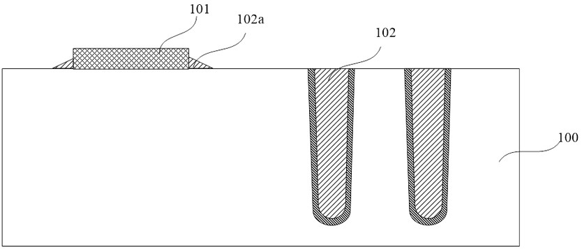
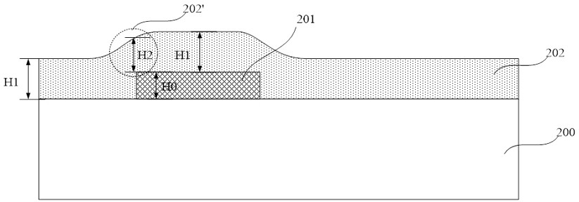
[0032] The following is attached figure 2 to attach Figure 8 The technical scheme proposed by the present invention is described in further detail with specific embodiments. The advantages and features of the present invention will become clearer from the following description. It should be noted that all the drawings are in a very simplified form and use imprecise scales, and are only used to facilitate and clearly assist the purpose of illustrating the embodiments of the present invention.

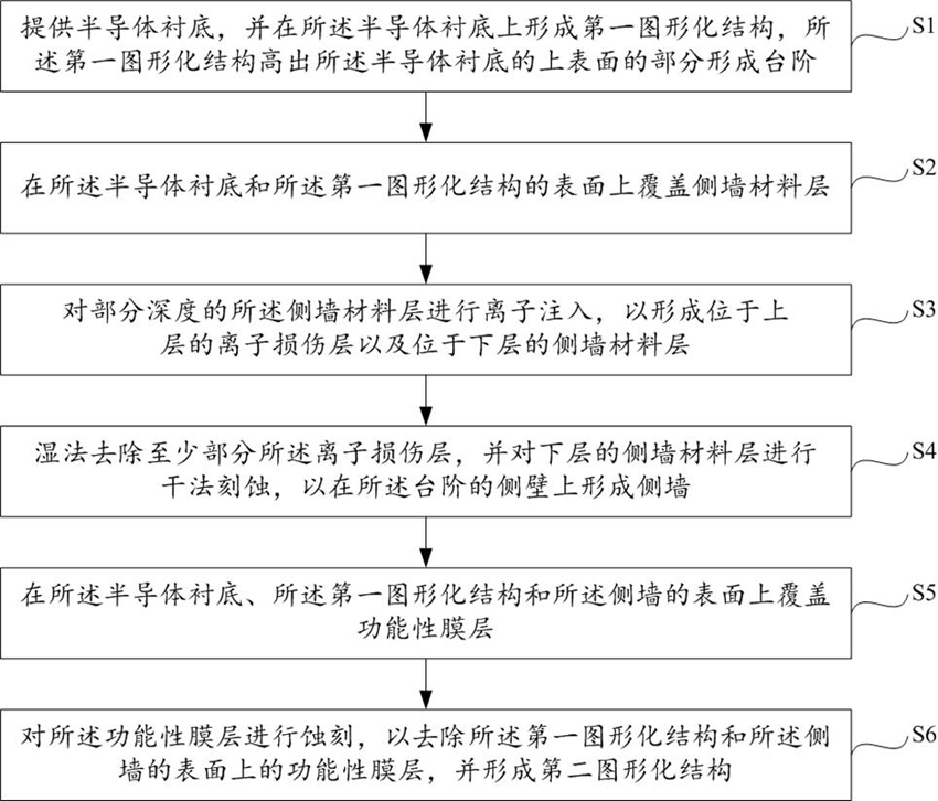
[0033] Please refer to figure 2 , an embodiment of the present invention provides a method for manufacturing a semiconductor device, comprising the following steps:

[0034] S1, providing a semiconductor substrate, and forming a first patterned structure on the semiconductor substrate, where a part of the first patterned structure higher than the upper surface of the semiconductor substrate forms a step;

[0035] S2, covering the surface of the semiconductor substrate and the firs...


PUM


Abstract

The invention provides a method for manufacturing a semiconductor device, which converts the upper layer of the side wall material layer into an ion damage layer by ion implantation, and the ion implantation dose at the top corner of the step is lower than that at other plane positions during ion implantation, so that After removing at least part of the ion damage layer by wet method, a relatively thick sidewall material layer can be retained on the top corner of the step, and after dry etching the remaining sidewall material layer, the sidewall formed on the sidewall of the step can be made The wall, while having a required height at its top, has a maximum width at its bottom extending along the surface of the semiconductor substrate, thereby reducing the aspect ratio of the formed sidewall. And because the aspect ratio of the formed sidewall is slower, it is more conducive to the etching and removal of the redundant film layer formed at the step in the subsequent process, avoiding the problem of etching residues formed on the sidewall of the step in the subsequent process, and thus improving the process caused by etching. The phenomenon of short-circuit failure of the device caused by the residue.

Description

technical field [0001] The invention relates to the technical field of integrated circuit manufacturing, in particular to a manufacturing method of a semiconductor device. Background technique [0002] With the increasing demand for miniaturization and integration of devices, special structures such as resistors and temperature sensors will be integrated in a chip, and polysilicon or metals (such as tungsten or Aluminum, etc.) or other materials such as silicon nitride, and patterned to form a step, due to the existence of the step, a thicker film layer will be deposited at the step position in the subsequent process, resulting in insufficient etching at the step position, resulting in etching residue. Specifically, such as figure 1 As shown, a film layer is formed on the surface of the substrate 100, and the film layer is further patterned to form patterned structures 101, and these patterned structures 101 form steps due to protruding from the surface of the substrate. D...

Claims


Application Information

Patent Timeline
Patent Type & Authority Patents(China)
IPC IPC(8): H01L21/8238
CPCH01L21/8238H01L21/823864
Inventor 王珏周旭钟志鸿
Owner SEMICON MFG ELECTRONICS (SHAOXING) CORP
Why Eureka
Try Eureka