
Image sensor and electronic equipment

An image sensor and pixel technology, applied in the image field, can solve the problem of low dynamic range of detectable light, achieve the effect of improving photosensitivity, increasing dynamic range, and increasing full well capacity

Active Publication Date: 2020-10-02
SHENZHEN GOODIX TECH CO LTD
View PDF14 Cites 1 Cited by
  • Summary
  • Abstract
  • Description
  • Claims
  • Application Information

AI Technical Summary

Problems solved by technology

[0005] The present application provides an image sensor and an electronic device aimed at solving the problem of low dynamic range of detectable light of a pixel unit

Method used


Image

  • Image sensor and electronic equipment
  • Image sensor and electronic equipment
  • Image sensor and electronic equipment

Examples


Embodiment Construction

[0035] In order to make the purpose, technical solution and advantages of the present application clearer, some embodiments of the present application will be further described in detail below in conjunction with the accompanying drawings and embodiments. It should be understood that the specific embodiments described here are only used to explain the present application, and are not intended to limit the present application.

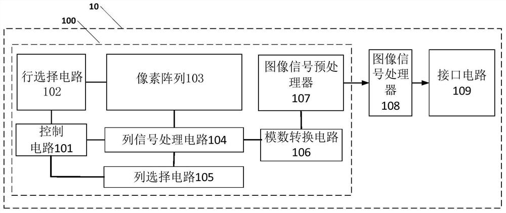
[0036] The image processing device uses the photoelectric conversion function of the pixel array to convert the optical image of the imaging object into an electrical signal proportional to the optical image, and then obtains the image of the imaging object. figure 1 A schematic block diagram of an image processing device 10 is shown, the image processing device 10 may refer to any electronic device, for example, the image processing device 10 may be a mobile phone; or, the image processing device 100 may also be a part of an electronic device For examp...


PUM


Abstract

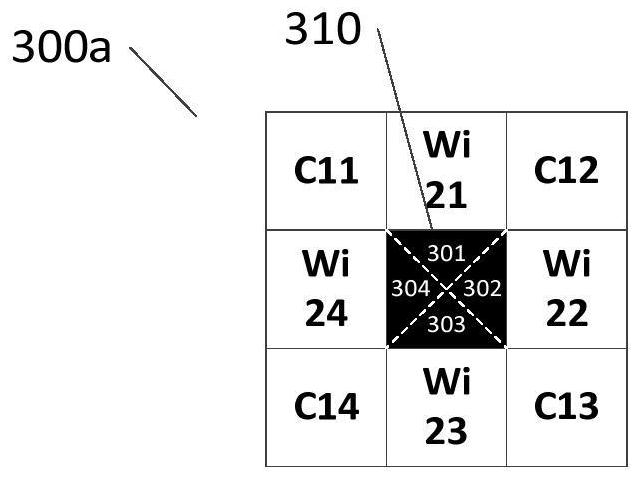
The embodiment of the invention relates to an image sensor and electronic equipment. The image sensor includes: a plurality of pixel unit groups, at least one pixel unit group comprises a color filterarray, wherein the color filter array comprises M first type filters, N second type filters and a light blocking area, the light blocking area comprises N light blocking sub-areas, and each light blocking sub-area is adjacent to the N second type filters; a pixel unit array positioned below the color filter array; wherein the pixel unit array comprises M first pixels and N second pixels, whereinthe M first pixels are in one-to-one correspondence with the M first type filters respectively, the N second pixels are in one-to-one correspondence with the N second type filters and the N light blocking sub-areas respectively, the area of the second pixels is larger than that of the first pixels, and M and N are integers larger than 0. According to the image sensor and the electronic equipment,the dynamic range of the image sensor is enlarged.

Description

technical field [0001] The embodiments of the present application relate to the image field, and more specifically, relate to an image sensor and an electronic device. Background technique [0002] A solid-state image sensor is a solid-state integrated component that converts optical image signals into digital signals. The solid-state image sensor includes a charge-coupled device (Charge-coupled Device, CCD) and a complementary metal oxide semiconductor (Complementary Metal Oxide Semiconductor, CMOS). Two types are widely used in consumer electronics, security monitoring, automotive electronics, and industrial manufacturing. [0003] The imaging principle of solid-state image sensors is based on the photoelectric conversion effect of semiconductor materials. A pixel array composed of a plurality of pixels is arranged on a semiconductor substrate, and each pixel contains a photoelectric conversion element and a readout circuit. When light is projected onto the pixel array, ...

Claims


Application Information

Patent Timeline
Patent Type & Authority Applications(China)
IPC IPC(8): H04N5/369H04N5/374
CPCH04N25/702H04N25/70H04N25/76
Inventor 姚国峰沈健
Owner SHENZHEN GOODIX TECH CO LTD
Learn More