Novel laser area array selective melting additive manufacturing process simulation method
An additive manufacturing and process simulation technology, applied in additive processing, 3D modeling, instruments, etc., can solve the problems of long scanning time and uneven stress distribution, and achieve the effect of improving processing efficiency, promoting development and reducing deformation.
- Summary
- Abstract
- Description
- Claims
- Application Information
AI Technical Summary
Problems solved by technology
Method used
Image
Examples
Embodiment 1
[0043] This embodiment provides a novel method for simulating a laser surface array selective fusion additive manufacturing process, and the specific steps are as follows:
[0044] Step 1. Design point source array
[0045] Under the condition of 200mm×200mm×25mm substrate, simulate the area array exposure area of 80mm×80mm, the size of the exposure area can be adjusted and optional in the simulation step; put 80×80 dot matrix spots in this area, and the density of dot matrix spots can be adjusted , The number is adjustable; the distance between each spot is 0.1mm-1mm, and the radius of a single spot heat source is 50μm-500μm.
[0046] This step needs to set the material properties and its thermophysical parameters.
[0047] Step 2, stl format file slice batch boundary extraction and grayscale processing
[0048] Export the designed 3D model as an stl format file, write a program to call the model for slice processing and output pictures of each layer, write a program to c...
Embodiment 2
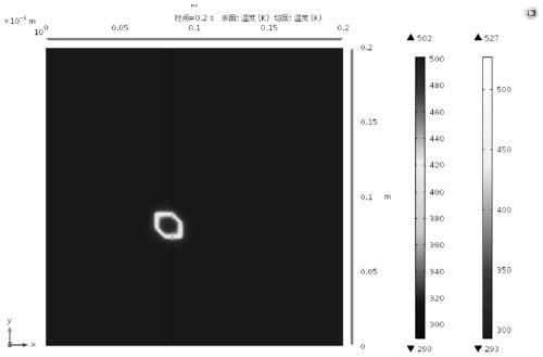
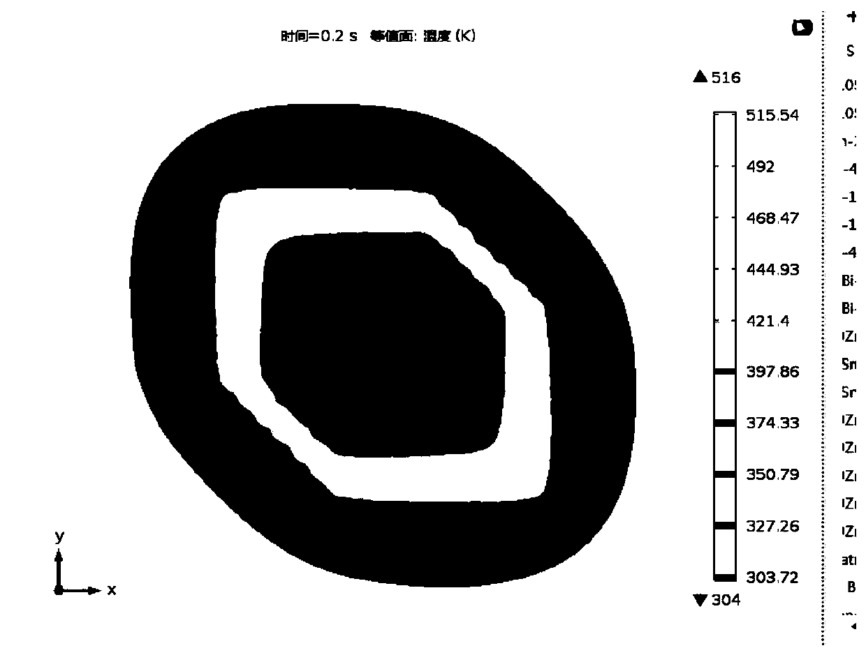
[0060] In this embodiment, taking the low-melting point metal Sn-9Zn alloy as an example, a simulated area-array exposure molten metal additive manufacturing experiment is carried out on a substrate with a length of 200 mm x a width of 200 mm x a height of 25 mm. This embodiment is used to illustrate the temperature field simulation process of custom spot shape, such as figure 1 with figure 2 shown.
[0061] First design the point source array. Create a substrate of 200mm×200mm×25mm, and create an area array exposure area of 80mm×80mm at the same time. The size of the exposure area can be adjusted and optional in the simulation step; an 80×80 array spot is placed in this area, and the density of the array point spot is adjustable and the number Adjustable; spot spacing 1mm, single spot heat source radius 500μm.
[0062] The substrate material is set as Sn-9Zn, and its thermophysical parameters are set to simulate the temperature field of processing Sn-9Zn alloy powder. ...
Embodiment 3
[0065] In this example, 6061 series aluminum alloy is taken as an example to simulate an area array exposure molten metal additive manufacturing experiment on a substrate with a length of 200 mm × width 200 mm × height 25 mm. This example is used to illustrate the role and effect of point source non-uniform regulation .
[0066] Design point source arrays. Create a substrate of 200mm×200mm×25mm, and create an area array exposure area of 80mm×80mm at the same time. The size of the exposure area can be adjusted and optional in the simulation step; an 80×80 array spot is placed in this area, and the density of the array point spot is adjustable and the number Adjustable; spot spacing 1mm, single spot heat source radius 500μm.
[0067] The substrate material is set to 6061 series aluminum alloy, and its thermophysical parameters are set to simulate the temperature field of processing 6061 aluminum alloy powder. In this embodiment, the simulated light spot pattern does not come...
PUM
 Abstract
Description
Claims
Application Information
 - R&D
- Intellectual Property
- Life Sciences
- Materials
- Tech Scout
- Unparalleled Data Quality
- Higher Quality Content
- 60% Fewer Hallucinations
Browse by: Latest US Patents, China's latest patents, Technical Efficacy Thesaurus, Application Domain, Technology Topic, Popular Technical Reports.
© 2025 PatSnap. All rights reserved.Legal|Privacy policy|Modern Slavery Act Transparency Statement|Sitemap|About US| Contact US: help@patsnap.com


