Semiconductor laser integrated with slow optical waveguide on chip

A laser and optical waveguide technology, which is applied in the direction of semiconductor lasers, optical waveguide semiconductor structures, lasers, etc., can solve problems such as poor device performance, increased optical field mode loss, and poor practicability, achieving low cost and expanding light output Aperture, the effect of reducing the divergence angle of the far field

Active Publication Date: 2020-07-31
XIDIAN UNIV
View PDF6 Cites 1 Cited by
  • Summary
  • Abstract
  • Description
  • Claims
  • Application Information

AI Technical Summary

Problems solved by technology

[0005] Most of these early researchers adopted the surface metal distribution feedback grating structure with simple structure and easy process to realize, so the optical field mode loss was significantly increased after the introduction of metal, and the performance of the device was generally poor, and continuous wave operation could not be realized.
In 2011, Yanbo Bai of Northwestern University in the United States adopted a buried two-stage annular cavity grating structure, see Bai, Y., etal.Applied Physics Letters, 2011.99(26):261104, this structure avoided the loss introduced by the metal, and successfully achieved a wavelength of 4.8μm , the surface-emitting quantum cascade laser of the annular cavity works in continuous wave CW at room temperature, but the far-field spot in this configuration presents a high-order annular pattern, which is not practical
Especially for strip cavity surface emitting quantum cascade lasers, the far field in the cavity length direction has been significantly improved, which is close to 0.1°, but this technology still has shortcomings in the ridge width direction, and the far field divergence angle is larger than that in the cavity length direction2 As many as an order of magnitude, showing an extremely compressed slit pattern
Therefore, the divergence in the ridge width direction has become a short board problem for the practical application of surface-emitting quantum cascade lasers

Method used


Image

  • Semiconductor laser integrated with slow optical waveguide on chip
  • Semiconductor laser integrated with slow optical waveguide on chip
  • Semiconductor laser integrated with slow optical waveguide on chip

Examples


Embodiment 1

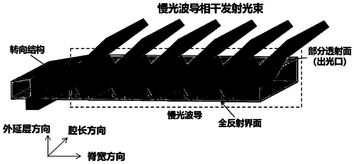
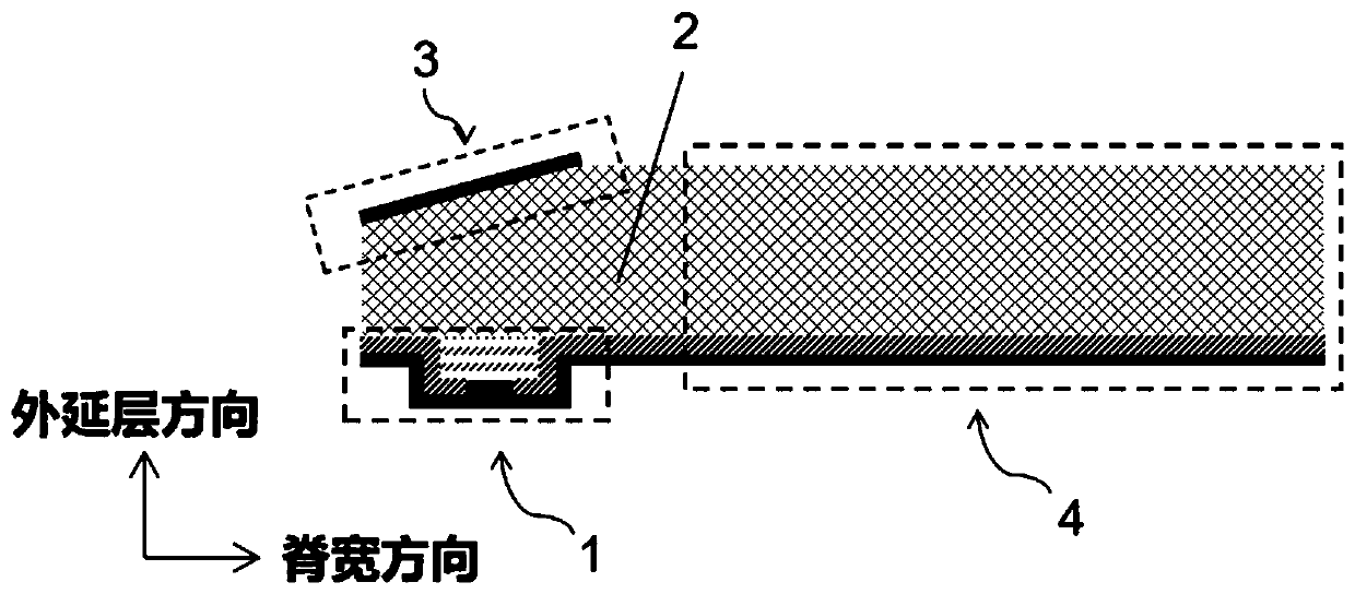
[0062] refer to Figure 10 , and combined with Figure 6 (a) and Figure 9 (a), in this example, the on-chip semiconductor laser with integrated slow light waveguide includes: laser active region 1, substrate 2, steering structure 3 and slow light waveguide structure 4. Wherein: the laser active region 1 is located on one side of the substrate 2 in the direction of the epitaxial layer, the steering structure 3 is located on the other side of the substrate in the direction of the epitaxial layer, and the slow optical waveguide structure 4 is located on the side of the substrate along the direction of the ridge width.

[0063] The laser active region 1 includes a ridge waveguide 11 , an electrical isolation layer 12 , a metal layer 14 and an electrical injection window 13 . Ridge waveguide 11 is the core area of ​​laser light emission, which is prepared by metal oxide chemical vapor deposition MOCVD or molecular beam epitaxy MBE equipment. According to the order of film depos...

Embodiment 2

[0071] refer to Figure 11 , and combined with Figure 6 (b) and Figure 9 (b), in this example, the on-chip semiconductor laser with integrated slow light waveguide includes: laser active region 1 and substrate 2, steering structure 3 and slow light waveguide structure 4. The laser active region 1 is located on one side of the epitaxial layer of the substrate 2, the steering structure 3 is located on the other side of the epitaxial layer of the substrate, and is symmetrically distributed with the laser active region structure relative to the substrate 2, and the slow optical waveguide Structure 4 is located on one side of the substrate along the ridge width direction.

[0072] The laser active region 1 includes a ridge waveguide 11 , an electrical isolation layer 12 , a metal layer 14 and an electrical injection window 13 . Ridge waveguide 11 is the core area of ​​laser light emission, which is prepared by metal oxide chemical vapor deposition MOCVD or molecular beam epita...

Embodiment 3

[0080] refer to Figure 12 , and combined with Figure 7 (a) and Figure 9 (a), the semiconductor laser integrated with slow light waveguide on chip in this example includes: laser active region 1, substrate 2, steering structure 3 and slow light waveguide structure 4. The laser active region 1 is located on one side of the substrate 2 in the direction of the epitaxial layer, the steering structure 3 is located on the other side of the substrate 2 in the direction of the epitaxial layer, and is symmetrical to the structure of the laser active region relative to the substrate 2, and the distribution of slow light The waveguide structure 4 is located on one side of the substrate 2 along the ridge width direction.

[0081] The laser active region 1 includes a ridge waveguide 11 , an electrical isolation layer 12 , a metal layer 14 and an electrical injection window 13 . Ridge waveguide 11 is the core area of ​​laser light emission, which is prepared by metal oxide chemical vap...


PUM


Abstract

The invention discloses a semiconductor laser integrated with a slow optical waveguide on a chip. The semiconductor laser mainly solves the problem of far-field divergence of outgoing beams of an existing semiconductor laser. The laser comprises a laser active region (1), a substrate (2), a steering structure (3) and a slow optical waveguide structure (4), the laser active region (1) is located onone side of the substrate (2) in the epitaxial layer direction, and the steering structure (3) is located on the other side of the substrate (2) in the epitaxial layer direction and used for changingthe propagation direction of laser beams vertically emitted by the laser active region; and the slow optical waveguide structure (4) is positioned on one side of the substrate (2) along the ridge width direction and is used for realizing emission of a coherent light beam array and reducing a far-field divergence angle of a light beam. According to the semiconductor laser, the far-field divergenceangle of the semiconductor laser can be greatly reduced, so that the system integration level of the semiconductor light source is improved, and the semiconductor laser can be used for laser infraredinterference, on-chip optical interconnection and space optical communication.

Description

technical field [0001] The invention belongs to the technical field of semiconductor optoelectronic devices, and in particular relates to a semiconductor laser, which can be used as a laser light source for photoelectric countermeasures, optical interconnection, optical communication, gas detection, and spectrum analysis. Background technique [0002] The mid-to-far infrared with a wave band of 3-12 μm is in great demand in the fields of national defense, environmental protection, medical treatment, and space optical communication due to its specific wavelength. Among many light source technologies, quantum cascade laser QCL has attracted much attention due to its advantages of miniaturization, integration and high performance. In the practical application of quantum cascade lasers, in order to ensure the energy concentration of the beam during propagation, combined with the working distance, the actual far-field divergence angle is less than 10mrad, that is, approximately 0...

Claims


Application Information

Patent Timeline
IPC IPC(8): H01S5/20H01S5/22H01S5/18H01S5/34
CPCH01S5/205H01S5/22H01S5/18H01S5/34
Inventor 姚丹阳张春福郝跃陈大正成亚楠
Owner XIDIAN UNIV
Why Eureka
Try Eureka