Radio frequency chip integrated packaging structure and producing method thereof

A technology of integrated packaging and radio frequency chips, applied in antenna support/mounting devices, semiconductor/solid-state device manufacturing, antennas, etc., can solve problems such as complex processes, inability to integrate antennas, difficulty in packaging radio frequency chips and antennas, etc., and achieve simple process , Reduce the size of the package, and improve the high-frequency electrical performance

Inactive Publication Date: 2020-07-24
NAT CENT FOR ADVANCED PACKAGING
View PDF6 Cites 24 Cited by
  • Summary
  • Abstract
  • Description
  • Claims
  • Application Information

AI Technical Summary

Problems solved by technology

[0003] The purpose of the present invention is to provide a radio frequency chip integrated packaging structure and its preparation method to solve the problem that the existing radio frequency chip and antenna are difficult to package
[0004] The purpose of the present invention is also to provide a radio frequency chip integrated packaging structure and its preparation method to solve the problem that the existing radio frequency chip and antenna are difficult to package
[0005] The object of the present invention is also to provide a radio frequency chip integrated packaging structure and its preparation method, to solve the problem that the existing radio frequency chip needs prefabricated metal frame, the process is complicated, and the problem that the antenna cannot be integrated

Method used


Image

  • Radio frequency chip integrated packaging structure and producing method thereof
  • Radio frequency chip integrated packaging structure and producing method thereof
  • Radio frequency chip integrated packaging structure and producing method thereof

Examples


Embodiment 1

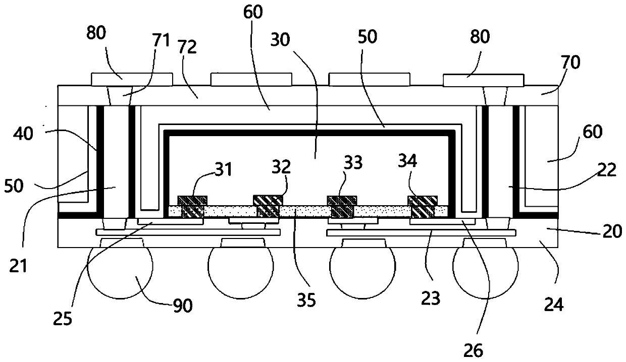
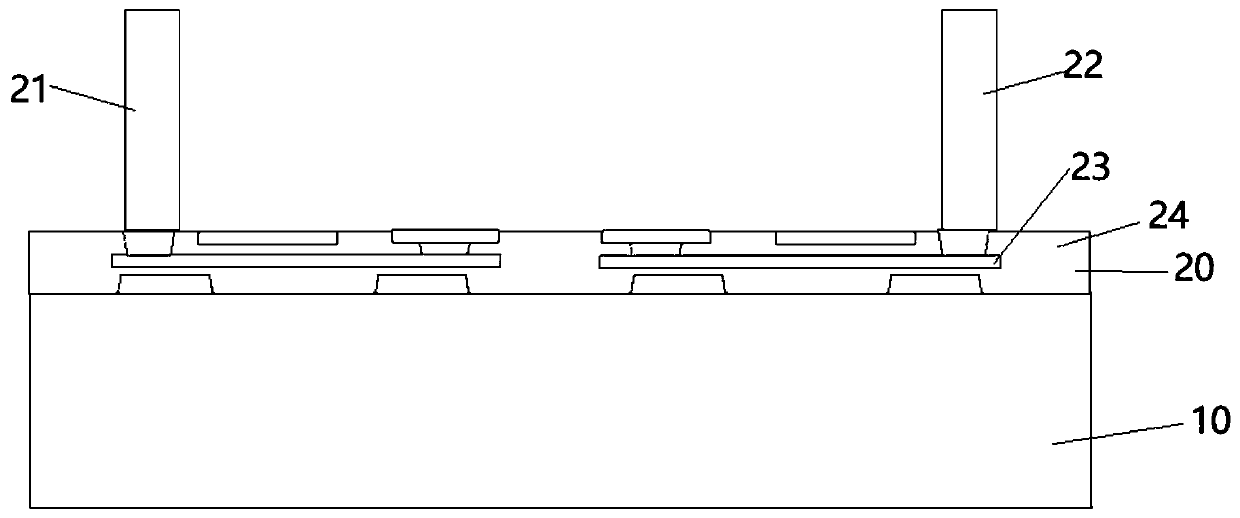
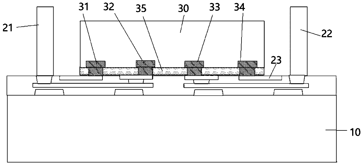
[0065] This embodiment also provides a radio frequency chip integrated packaging structure, such as figure 1 As shown, the integrated package structure of the radio frequency chip includes: a first conductive layer 20; one or more conductive columns (such as figure 1 As shown, the example is the first conductive column 21 and the second conductive column 22), which stand on the first conductive layer 20; the radio frequency chip 30 is attached (for example, bonded) on the first conductive layer 20, The radio frequency chip 30 is located between the first conductive column 21 and the second conductive column 22; the grounding parts 25 and 26 of the shielding layer are located between the first conductive column 21, the second conductive column 22 and the On the first conductive layer 20 between the radio frequency chips 30; the insulating film 40 covers the radio frequency chip 30, the sides of the first conductive pillars 21 and the sides of the second conductive pillars 22, a...

Embodiment 2

[0073] This embodiment provides the preparation method of the radio frequency chip integrated packaging structure in the previous embodiment, such as Figure 2-9As shown, the preparation method of the radio frequency chip integrated package structure includes: providing a temporary bonding carrier 10, forming a first conductive layer 20 on the first surface of the temporary bonding carrier 10, and forming a first conductive layer 20 on the first conductive layer Form the first conductive column 21 and the second conductive column 22 on the 20; attach the radio frequency chip 30 to the first conductive layer 20, the radio frequency chip 30 is located on the first conductive column 21 and the second conductive layer between the pillars 22; form an insulating film 40, the insulating film 40 covers the first conductive layer 20, the radio frequency chip 30, the first conductive pillar 21 and the second conductive pillar 22; remove the first conductive pillar Part of the insulating...

Embodiment 3

[0086] This embodiment provides the preparation method of the radio frequency chip integrated packaging structure in the previous embodiment, such as Figure 10 As shown, in the preparation method of the radio frequency chip integrated packaging structure described in the previous embodiment, arranging the antenna array 80 on the second conductive layer 70 includes: arranging the first antenna array on the second conductive layer 70 81, forming an antenna plastic layer 83, the antenna plastic layer 83 covers the first antenna array 81, and adopts a compression molding process, a transfer molding process, a liquid sealing molding process, a vacuum lamination process, or a spin coating process to form the antenna Plastic sealing layer 83 ; the material of the antenna plastic sealing layer 83 may include one of polyimide, silica gel, and epoxy resin. The plastic sealing layer of the antenna may also include one or more of low dielectric constant materials such as polytetrafluoroe...


PUM


Abstract

The invention provides a radio frequency chip integrated packaging structure and a producing method thereof. The producing method of the radio frequency chip integrated packaging structure comprises the steps: forming a first conductive layer on a first surface of a temporary bonding carrier plate, and forming one or more conductive columns on the first conductive layer; attaching a chip to the first conductive layer; forming an insulating film, wherein the insulating film covers the first conductive layer, the chip and the one or more conductive columns; removing part of the insulating film,exposing part of a conductive circuit of the first conductive layer, and forming a shielding layer grounding position; forming a shielding layer which covers the insulating film and is electrically connected with the shielding layer grounding position; forming a plastic package layer, wherein the plastic package layer covers the shielding layer; exposing top surfaces of the one or more conductivecolumns; forming a second conductive layer on the top surface of the plastic package layer, wherein the second conductive layer is electrically connected with the one or more conductive columns; and arranging an antenna array on the second conductive layer.

Description

technical field [0001] The invention relates to the technical field of semiconductor packaging, in particular to a radio frequency chip integrated packaging structure and a preparation method thereof. Background technique [0002] Lower cost, more reliable, faster and higher density circuits are the goals pursued by integrated circuit packaging. In the future, integrated circuit packaging will increase the integration density of various electronic components by continuously reducing the minimum feature size. Currently, advanced packaging methods include: Wafer Level Chip Scale Packaging (WLCSP), Fan-Out Wafer Level Package (FOWLP), Flip Chip, Package on Package (Package on Package, POP) and so on. Fan-out wafer-level packaging is an embedded chip packaging method for wafer-level processing. It is currently one of the advanced packaging methods with more input / output ports (I / O) and better integration flexibility. Compared with conventional wafer-level packaging, fan-out w...

Claims


Application Information

Patent Timeline
Patent Type & Authority Applications(China)
IPC IPC(8): H01L21/48H01L21/60H01L23/552H01L23/66H01Q1/22H01Q1/52
CPCH01L21/4853H01L21/4857H01L21/486H01L23/552H01L23/66H01L24/81H01L2223/6677H01L2224/81005H01Q1/2283H01Q1/526H01L2224/18
Inventor 王全龙曹立强陈峰孙绪燕
Owner NAT CENT FOR ADVANCED PACKAGING
Why Eureka
Try Eureka