Double-shell asymmetric semiconductor material and super-assembly method thereof

An assembly method, asymmetric technology, applied in chemical instruments and methods, nanotechnology for materials and surface science, other chemical processes, etc., can solve problems such as speed needs to be improved, limited motor application range, etc., to achieve transmission and separation. Efficiency improvement, photoelectric conversion efficiency improvement, wide pore size distribution effect

Pending Publication Date: 2020-06-19
FUDAN UNIV
View PDF12 Cites 1 Cited by
  • Summary
  • Abstract
  • Description
  • Claims
  • Application Information

AI Technical Summary

Problems solved by technology

due to H 2 o 2 and ultraviolet light are biologically toxic, which greatly limits the application range of the motor
h 2 O is an ideal fuel, but the speed of light-driven micro-nano motors fueled by pure water still needs to be improved

Method used


Image

  • Double-shell asymmetric semiconductor material and super-assembly method thereof
  • Double-shell asymmetric semiconductor material and super-assembly method thereof
  • Double-shell asymmetric semiconductor material and super-assembly method thereof

Examples


Embodiment 1

[0028] This embodiment provides a double-shell asymmetric semiconductor material and its super-assembly method.

[0029] The superassembly method of double-shell asymmetric semiconductor materials includes the following steps:

[0030] Step 1: Asymmetric bottle-shaped open carbon polymer frameworks (VPFs for short) were prepared by microemulsion template method in a hydrothermal environment.

[0031] Its specific process includes:

[0032] In step S1-1, the template agent is first dissolved in deionized water, and stirred until it becomes a clear solution, that is, a uniform microemulsion system is formed. Among them, the templating agent is composed of triblock copolymer PEO 20 -PPO 70 -PEO 20 (referred to as P123) and sodium salt self-assembled, the sodium salt is any one of sodium oleate (SO), sodium stearate, sodium laurate, and the molar ratio of P123 and sodium salt is 1: (2- 32), the molar mass ratio of template agent to water is 0.1275mmol: (40mL-100mL). In this ...

Embodiment 2

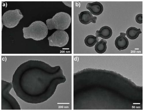
[0046] This example is the double-shell asymmetric TiO prepared in Example 1 2 @TiO 2 Semiconductor materials and hollow TiO 2 The nanospheres were compared in terms of structure, ultraviolet absorption, photocurrent performance, and motion performance in water.

[0047] 1. Structure

[0048] Figure 4 : It is hollow TiO in embodiment 2 of the present invention 2 Electron micrographs of nanospheres, wherein (a-b) is transmission electron micrographs; Figure 5 : It is double-shell asymmetric TiO in embodiment 2 of the present invention 2 @TiO 2 XRD diffraction patterns of semiconductor materials and hollow TiO2 nanospheres.

[0049] From Figure 4 It can be seen that the prepared hollow TiO 2 The size of the nanosphere is uniform, and it is a hollow and closed single-shell structure. The thickness of the shell layer is about 40nm, and the diameter is about 500nm. From Figure 5 As can be seen in the hollow TiO 2 Nanospheres and double-shell asymmetric TiO 2 @TiO ...


PUM

PropertyMeasurementUnit
thicknessaaaaaaaaaa
lengthaaaaaaaaaa
sizeaaaaaaaaaa

Abstract

The invention provides a double-shell asymmetric semiconductor material and a super-assembly method thereof. The method comprises the following steps: 1, dissolving a template agent in water to form auniform microemulsion system, adding a carbon source, fully mixing and stirring, putting the obtained mixed solution into a reaction kettle, and reacting in an oven at 140-160 DEG C for 8-24 hours toobtain an asymmetric bottle-shaped open carbon polymer framework (VPFs), 2, by taking VPFs as a template and uniformly growing amorphous TiO2 layers on the outer surface and the inner surface of thetemplate to obtain an intermediate of a sandwich structure and 3, calcining the intermediate to remove a bottle-shaped open carbon polymer framework, thereby obtaining the double-shell asymmetric semiconductor material, wherein the step 2 comprises the following sub-steps: dispersing VPFs in ethanol, then adding ammonia water and tetrabutyl titanate, and putting the mixture into an oil bath pot at25-80 DEG C to react for 12-30 hours to obtain the intermediate.

Description

technical field [0001] The invention belongs to the field of materials and artificial micro-nano motors, and in particular relates to a double-shell asymmetric semiconductor material and a super-assembly method thereof. Background technique [0002] TiO 2 It is one of the most widely studied semiconductor oxides. As a typical n-type semiconductor material, TiO 2 Due to the advantages of non-toxicity, good stability, low cost, large surface area, large pore volume, and excellent photoelectric performance, it has become a high-profile photocatalyst. It has a wide range of applications in many energy and environmental fields such as catalytic degradation, sterilization and disinfection, and photolysis of water to produce hydrogen. TiO 2 The photocatalytic performance of the catalyst depends largely on the morphology of the catalyst. So far, nano-TiO 2 Great progress has been made in the preparation of materials. Among various morphologies, TiO with multi-shell hollow stru...

Claims


Application Information

Patent Timeline
Patent Type & Authority Applications(China)
IPC IPC(8): C01G23/053B82Y40/00B82Y30/00B01J21/06B01J20/06B01J20/30
CPCC01G23/053B82Y40/00B82Y30/00B01J20/06B01J21/063B01J35/004C01P2002/72C01P2004/03C01P2004/04C01P2002/84B01J2220/4812
Inventor 孔彪曾洁谢磊刘天亿
Owner FUDAN UNIV
Why Eureka
Try Eureka