Fingerprint acquisition device and manufacturing method thereof

A fingerprint collection and production method technology, applied in the direction of instruments, character and pattern recognition, computer components, etc., can solve the problems of high cost, thick modules, complex structure, etc., and achieve the effect of improving stability

Pending Publication Date: 2020-05-29
SHANGHAI HARVEST INTELLIGENCE TECH CO LTD
View PDF6 Cites 0 Cited by
  • Summary
  • Abstract
  • Description
  • Claims
  • Application Information

AI Technical Summary

Problems solved by technology

[0004] Existing optical fingerprint recognition technologies are basically based on the imaging principle of geometric optical lenses. The fingerprint modules used include microlens arrays, optical spatial filters and other components, which have complex structures, thick modules, small sensing ranges, and high costs. many shortcomings

Method used


Image

  • Fingerprint acquisition device and manufacturing method thereof
  • Fingerprint acquisition device and manufacturing method thereof
  • Fingerprint acquisition device and manufacturing method thereof

Examples


Embodiment Construction

[0037] In order to make the above objects, features and beneficial effects of the present invention more comprehensible, specific embodiments of the present invention will be described in detail below in conjunction with the accompanying drawings. Each embodiment in this specification is described in a progressive manner, each embodiment focuses on the difference from other embodiments, and the same or similar parts of each embodiment can be referred to each other.

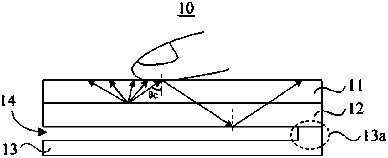
[0038] refer to figure 1 , figure 1 It is a schematic structural diagram of a fingerprint collection device 10 . The fingerprint collection device 10 is an off-screen optical fingerprint recognition technology that utilizes the total reflection imaging principle of physical optics to realize lightless collimation (for example: no lens). The fingerprint collection device 10 sequentially includes along its thickness direction: a light-transmitting cover plate 11 , a display layer 12 , and a sensing module 13 . Wh...


PUM

PropertyMeasurementUnit
thicknessaaaaaaaaaa
refractive indexaaaaaaaaaa

Abstract

The invention provides a fingerprint acquisition device and a manufacturing method thereof. The fingerprint acquisition device comprises a light-transmitting cover plate, a display layer, a dielectricfilm and a sensing module, wherein the light-transmitting cover plate is provided with a first surface for contacting a fingerprint; the display layer is arranged on the second surface of the light-transmitting cover plate and comprises a pixel array for displaying; the first surface of the sensing module is provided with a protruding part;the dielectric film is filled between the display layer and the area, not provided with the protruding part, of the first surface of the sensing module, the two surfaces of the dielectric film in the thickness direction are attached to the display layer andthe sensing module respectively, the dielectric film is pervious to light, and the difference value between the refractive index of the dielectric film and the refractive index of the display layer is within a preset range. According to the fingerprint acquisition device and the manufacturing method thereof provided by the embodiment of the invention, a gap between the display layer and the sensing module due to the existence of the convex part can be avoided, the normal reception of fingerprint reflection light rays by the sensing module is ensured, the noise is reduced, and the stability isimproved.

Description

technical field [0001] The invention relates to the technical field of fingerprint identification, in particular to a fingerprint collection device and a manufacturing method thereof. Background technique [0002] Fingerprint imaging recognition technology is to transmit a detection signal to the fingerprint through the emission source, and then use the sensor to collect the detection signal modulated by the fingerprint, and then perform data processing on the collected signal to obtain the fingerprint image. Due to the uniqueness of human fingerprints, fingerprint imaging recognition technology has been widely used in various fields. Examples include security check areas, access control systems, or the unlocking of devices such as PCs and mobile phones. [0003] There are many ways to implement the fingerprint imaging recognition technology, such as optical imaging, capacitive imaging, or ultrasonic imaging. Relatively speaking, optical fingerprint imaging recognition tec...

Claims


Application Information

Patent Timeline
Patent Type & Authority Applications(China)
IPC IPC(8): G06K9/00
CPCG06V40/1324
Inventor 王天洋汪菲胡雪珂冯胜顾凤军黄建东
Owner SHANGHAI HARVEST INTELLIGENCE TECH CO LTD
Why Eureka
Try Eureka