Chip and antenna integrated three-dimensional packaging structure and preparation method thereof

A three-dimensional packaging and chip technology, which is applied in the structural form of radiation elements, semiconductor/solid-state device manufacturing, electrical components, etc., can solve the problems of large packaging volume, poor integration, and large loss, and achieve high integration performance, low cost, and low loss. low effect

Pending Publication Date: 2020-05-26
XIAMEN SKY SEMICON TECH CO LTD
View PDF0 Cites 3 Cited by
  • Summary
  • Abstract
  • Description
  • Claims
  • Application Information

AI Technical Summary

Problems solved by technology

[0003] Traditional antennas are usually assembled on a PCB with a millimeter-wave chip in a two-dimensional plane, so the package has a large volume, large area, poor integration, and large loss under millimeter-wave transmission.

Method used


Image

  • Chip and antenna integrated three-dimensional packaging structure and preparation method thereof
  • Chip and antenna integrated three-dimensional packaging structure and preparation method thereof
  • Chip and antenna integrated three-dimensional packaging structure and preparation method thereof

Examples


Embodiment 1

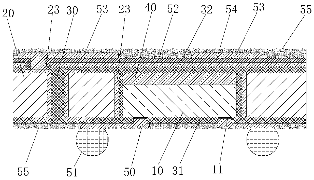
[0043] see figure 1 , a chip and antenna integrated three-dimensional packaging structure, including at least one chip 10 and a glass substrate 20 . The chip 10 has a first surface and a second surface, the first surface is provided with functional areas and electrodes 11, and the second surface is opposite to the first surface. The chip 10 of the present invention is mainly a millimeter-wave chip, which includes gallium arsenide (GaAs), InP (indium phosphide) millimeter-wave chips, gallium nitride (GaN) millimeter-wave chips, and the like.

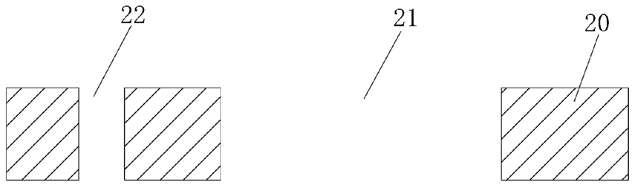
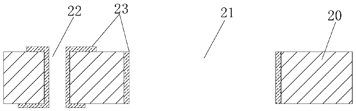
[0044] At least one through groove 21 and at least one through hole 22 are arranged on the glass substrate 20, and there is a distance between the through groove 21 and the through hole 22. The number of through grooves 21 can be one, two or even more, and the number of through holes 22 The quantity can be one, two, three or even more.

[0045] Metal conductive material 23 is deposited on the inner wall of the through groove 21 and the ...

Embodiment 2

[0063] see Figure 8 , a chip and antenna integrated three-dimensional packaging structure and its preparation method, its main features are the same as the first embodiment, the difference is that no passivation layer is provided on the surface of the antenna layer 53 and the exposed surface of the insulating layer 54. In the corresponding preparation method, the step of forming a passivation layer on the surface of the antenna layer 53 and the exposed surface of the insulating layer 54 is not included.


PUM


Abstract

The invention relates to a chip and antenna integrated three-dimensional packaging structure and a preparation method thereof. The chip and antenna integrated three-dimensional packaging structure comprises at least one chip, wherein the chip is provided with a first surface and a second surface, and the first surface is provided with a functional area and an electrode. The chip and antenna integrated three-dimensional packaging structure also comprises a glass substrate, wherein at least one through groove and at least one through hole are arranged on the glass substrate, and a metal conductive material is deposited in the inner walls of the through groove and the through hole; the chip and a heat dissipation metal block are embedded in the through groove through a bonding structure, andthe heat dissipation metal block is located on the second surface of the chip; the bonding structure is also filled in the through hole, a first wiring surface is formed on the first surface of the chip and one surface of the glass substrate, and a second wiring surface is formed on the surface of the heat dissipation metal block and the other surface of the glass substrate; the first wiring surface is provided with at least one metal circuit to be electrically connected with the electrode of the chip; the second wiring surface is provided with at least one grounding layer and at least one antenna layer, and the antenna layer is electrically connected with the metal conductive material on the through hole. The three-dimensional packaging structure has the advantages of compact structure, thin packaging thickness, short signal transmission line, low loss and high electrical property.

Description

technical field [0001] The invention relates to the field of semiconductor packaging, in particular to a three-dimensional packaging structure integrating a chip and an antenna and a preparation method thereof. Background technique [0002] With the development of high-frequency electronic products towards high speed and miniaturization, the industry has brought vertical stack packaging solutions to mainstream applications such as portable equipment, entertainment and automobiles. [0003] Traditional antennas are usually assembled on a PCB with a millimeter-wave chip in a two-dimensional plane, so the package has a large volume, large area, poor integration, and large loss under millimeter-wave transmission. [0004] Therefore, in order to reduce the circuit board area occupied by the antenna, arrange the packaging structure reasonably, and improve the overall antenna packaging efficiency and antenna performance, a high-performance, compact and fully integrated antenna pack...

Claims


Application Information

Patent Timeline
Patent Type & Authority Applications(China)
IPC IPC(8): H01L23/66H01L23/31H01L23/367H01L21/50H01Q1/38
CPCH01L21/50H01L23/3107H01L23/367H01L23/66H01L2223/6677H01Q1/38H01L2224/18
Inventor 于大全
Owner XIAMEN SKY SEMICON TECH CO LTD
Why Eureka
Try Eureka