Silicon structure with patterned surface and preparation method thereof and solar cell

A patterned surface and silicon structure technology, which is applied in the field of solar cells, can solve the problems of the photoelectric conversion efficiency of solar cells, etc., and achieve the effect of expanding the scope of application

Active Publication Date: 2020-05-22
苏州纳捷森光电技术有限公司
View PDF8 Cites 2 Cited by
  • Summary
  • Abstract
  • Description
  • Claims
  • Application Information

AI Technical Summary

Problems solved by technology

In the prior art, graphics are depicted by covering the solar cells with patterned translucent filter films. However, in this way, the filter films themselves will absorb and reflect a large amount of visible light, which will lead to light- The power conversion efficiency drops significantly

Method used


Image

  • Silicon structure with patterned surface and preparation method thereof and solar cell
  • Silicon structure with patterned surface and preparation method thereof and solar cell
  • Silicon structure with patterned surface and preparation method thereof and solar cell

Examples


Embodiment Construction

[0044] figure 1 A schematic structural diagram of a preset pattern according to an embodiment of the present invention is shown. figure 2 A schematic structural view of a silicon structure 1 with a patterned surface according to an embodiment of the present invention is shown. combine figure 1 with figure 2 It can be seen that the pattern on the surface of the silicon structure 1 is visually consistent with the preset pattern.

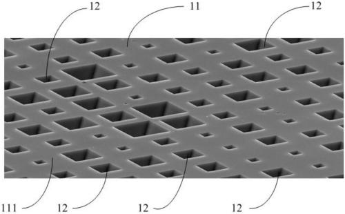
[0045] image 3 show figure 2 A partial scanning electron microscope image of the silicon structure 1 shown. The silicon structure 1 includes a silicon substrate 11 and various silicon microstructures. The silicon substrate 11 has a first surface 111 and a second surface (not shown) opposite to the first surface 111 . A variety of silicon microstructures have different reflectivity, and each silicon microstructure includes a plurality of silicon microunits 12 with the same reflectivity, each silicon microunit 12 is constructed on the silicon ...


PUM


Abstract

The invention provides a silicon structure with a patterned surface and a preparation method thereof and a solar cell. The silicon structure comprises: a silicon substrate having a first surface and asecond surface opposite to the first surface; a plurality of silicon microstructures which have different reflectivity, wherein each silicon microstructure comprises a plurality of silicon microunitswith the same reflectivity, and each silicon microunit is constructed on the silicon substrate and etched for a preset depth from the first surface of the silicon substrate to the direction close tothe second surface of the silicon substrate, the number of each silicon microstructure and the arrangement mode of all the silicon micro-units on the silicon substrate are determined according to a preset pattern, so that the pattern formed by all the silicon micro-units is visually consistent with the preset pattern. According to the scheme provided by the invention, any grayscale image can be drawn on the silicon solar cell panel on the premise of not losing obvious optical-electric conversion performance.

Description

technical field [0001] The invention relates to the field of designing semiconductor devices, in particular to a silicon structure with a patterned surface, a preparation method and a solar cell. Background technique [0002] With the gradual popularization of distributed photovoltaic energy, solar cells have gradually begun to be applied on a large scale in the construction of cities and towns, such as laying solar panels on roofs or roads to form part of the urban energy system. In addition, it can also be integrated in some low-power portable electronic devices, such as solar-powered watches, calculators, etc. [0003] Since the cost of solar power generation is still higher than that of traditional energy sources, the current research direction on solar cells is still focused on improving the photoelectric conversion efficiency of solar cells and reducing the cost of cells. In order to absorb as much available light as possible, traditional silicon-based solar cells are...

Claims


Application Information

Patent Timeline
IPC IPC(8): H01L31/0236H01L31/18
CPCH01L31/02363H01L31/1804Y02E10/547Y02P70/50
Inventor 揭建胜丁可张秀娟
Owner 苏州纳捷森光电技术有限公司
Why Eureka
Try Eureka