A non-uniformity correction circuit for apd detector array
A non-uniformity correction and APD array technology, applied in the field of APD detectors, can solve problems such as difficult integration, high power consumption, and inability to completely avoid non-uniformity, and achieve the effect of small system scale and low power consumption
- Summary
- Abstract
- Description
- Claims
- Application Information
AI Technical Summary
Problems solved by technology
Method used
Image

Examples
Embodiment 1
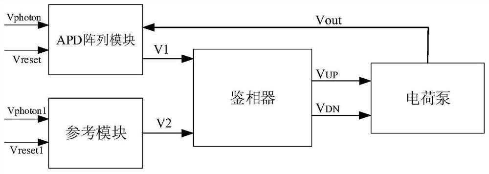
[0044] See figure 1 , figure 1 A schematic structural diagram of a non-uniformity correction circuit for an APD detector array provided by an embodiment of the present invention. This embodiment provides a non-uniformity correction circuit for an APD detector array, the correction circuit includes an APD array module, a reference module, a phase detector, and a charge pump, wherein,
[0045] The APD array module is used to perform current sensing and shaping processing on the second input signal to obtain the first digital signal after performing reset processing according to the first input signal;
[0046] The reference module is configured to perform current sensing and shaping processing on the fourth input signal to obtain the second digital signal after performing reset processing according to the third input signal;
[0047] The phase detector is connected to the APD array module and the reference module, and is used to compare the phase difference between the first d...
Embodiment 2
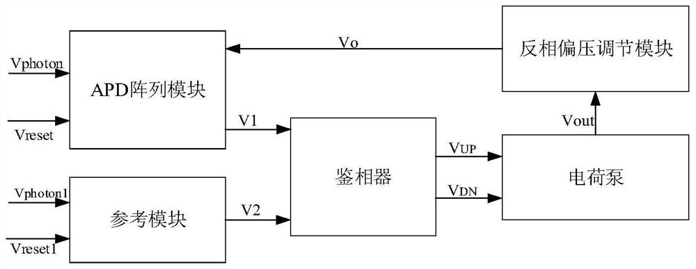
[0064] On the basis of the first embodiment above, please refer to image 3 , image 3 A schematic structural diagram of another non-uniformity correction circuit for an APD detector array provided by the embodiment of the present invention. It can be seen that this embodiment is based on the non-uniformity correction circuit for an APD detector array provided in the first embodiment above. , also includes a reverse bias voltage regulation module.
[0065] Specifically, the reverse bias adjustment module in this embodiment is connected to the charge pump and the APD array module, and is used to buffer the first processing signal to obtain the second processing signal Vo, and input the second processing signal to the APD array module . Since the first processing signal Vout output by the charge pump has no large current drive capability, if the output voltage of the charge pump is directly connected to the anode of the APD array unit, the output voltage of the charge pump may...
Embodiment 3
[0073] On the basis of the above-mentioned embodiment 2, the circuit of each APD array unit, reference module, phase detector, charge pump, and reverse bias voltage adjustment module in the APD array module is designed in detail as follows in this embodiment, but not limited Based on this design, it is further illustrated that the non-uniformity correction circuit oriented to the APD detector array provided by this embodiment can solve the problem of non-uniformity of the traditional APD array, and the correction circuit of this embodiment is composed of modules such as a phase detector and a charge pump. The system is small in scale and low in power consumption, and can realize monolithic integration with a large array of APDs, specifically:
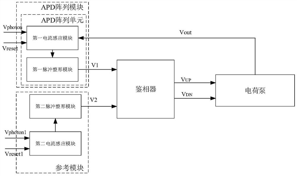
[0074] See Figure 5 , Figure 5 A schematic circuit diagram of an APD array unit in an APD detector array-oriented non-uniformity correction circuit provided for an embodiment of the present invention. In this embodiment, each APD array...
PUM
 Abstract
Description
Claims
Application Information
 - Generate Ideas
- Intellectual Property
- Life Sciences
- Materials
- Tech Scout
- Unparalleled Data Quality
- Higher Quality Content
- 60% Fewer Hallucinations
Browse by: Latest US Patents, China's latest patents, Technical Efficacy Thesaurus, Application Domain, Technology Topic, Popular Technical Reports.
© 2025 PatSnap. All rights reserved.Legal|Privacy policy|Modern Slavery Act Transparency Statement|Sitemap|About US| Contact US: help@patsnap.com