Organic memory and preparation method thereof
An organic memory and organic storage technology, applied in the field of optoelectronics, to achieve the effects of simple preparation process, small and portable, and functional integration.
- Summary
- Abstract
- Description
- Claims
- Application Information
AI Technical Summary
Problems solved by technology
Method used
Image
Examples
Embodiment 1
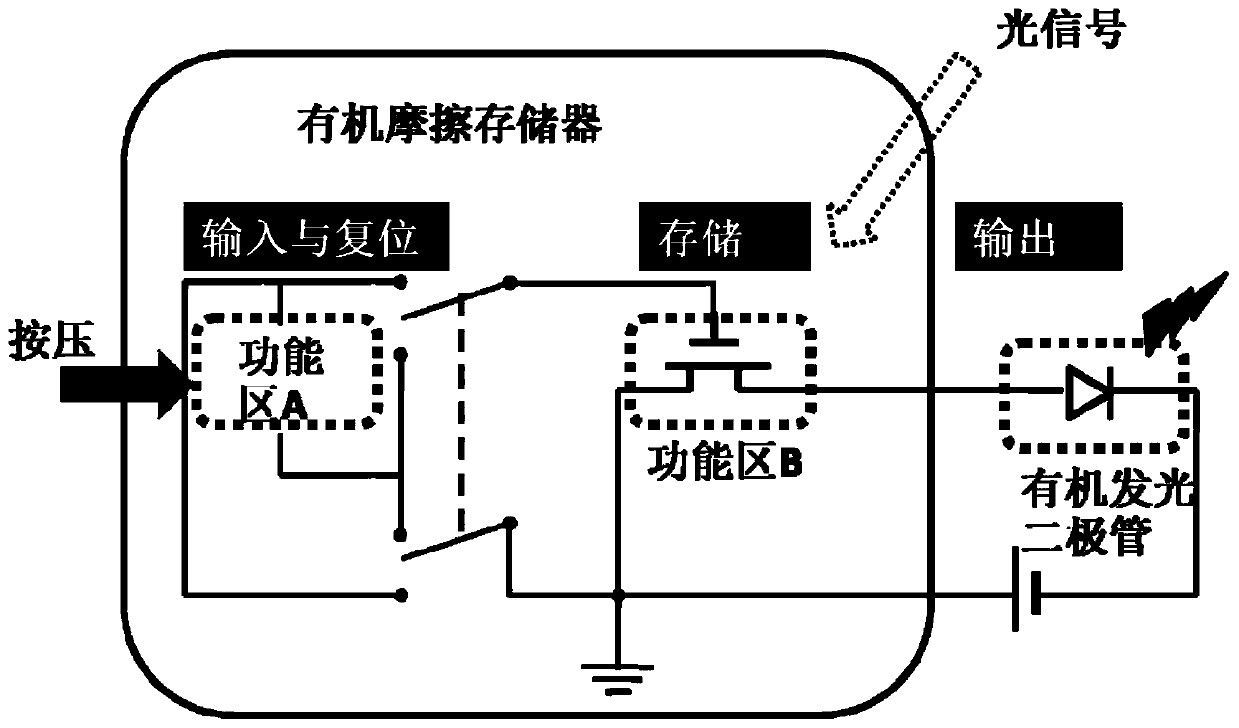
[0026] The organic friction memory structure schematic diagram of the present invention is as attached figure 1 As shown, including functional area A and functional area B. Functional area A is the triboelectric generation layer, and functional area B is the organic storage layer. The two electrode layers of the triboelectric layer are respectively connected to the gate and the source of the organic storage layer, and the left and right figures show the two connection modes.
[0027] Functional area A The triboelectric layer has two substrates, two electrodes, and two friction layers (one of the friction layers can be an electrode at the same time), such as figure 2 shown.
[0028] 21 and 26 are substrates, which can be hard substrates, such as plexiglass, or flexible substrates, such as polyethylene terephthalate PET;
[0029] 22 and 25 are electrode layers, and its material can adopt Cu etc.;
[0030] 23 and 24 are friction layers, and its material can be selected from ...
Embodiment 2
[0040] Figure 4 It is a schematic diagram of the organic photosensitive storage layer in functional area B, including a substrate with a gate electrode, a source electrode and a drain electrode, an insulating layer, and an organic photosensitive semiconductor layer.
[0041] 41 is a substrate with a gate electrode, which may be a glass substrate coated with ITO or a flexible substrate coated with ITO, such as a PET substrate.
[0042] 42 is an insulating layer, which can be polymer material polymethyl methacrylate (PMMA), or metal oxide, such as tantalum pentoxide Ta2O5;
[0043] 43 is an organic photosensitive semiconductor layer, which can use pentacene, etc.;
[0044] 44 is a source electrode and a drain electrode, metals such as gold and silver, or transparent electrode materials such as ITO can be used;
Embodiment 3
[0046] Figure 5 It is the pressing storage characteristic of the floating gate structure organic friction memory, and its working principle is as follows (take P-type semiconductor, floating gate captures electrons as an example):
[0047] When there is no external force, the friction layers are separated from each other, and the voltage between the gate and the source is zero at this time. When there is an external force, the friction layers touch and rub against each other. Due to the electrostatic effect, one layer has a positive charge and the other layer has a negative charge, generating electrostatic potential energy. At this time, it is equivalent to applying a positive gate to the memory layer. Electrode voltage, under the action of this positive electric field, electrons in the semiconductor enter the floating gate layer and are trapped, leaving excess holes in the semiconductor, the channel current rises, and the signal writing is realized, and the current curve shi...
PUM
 Abstract
Description
Claims
Application Information
 - Generate Ideas
- Intellectual Property
- Life Sciences
- Materials
- Tech Scout
- Unparalleled Data Quality
- Higher Quality Content
- 60% Fewer Hallucinations
Browse by: Latest US Patents, China's latest patents, Technical Efficacy Thesaurus, Application Domain, Technology Topic, Popular Technical Reports.
© 2025 PatSnap. All rights reserved.Legal|Privacy policy|Modern Slavery Act Transparency Statement|Sitemap|About US| Contact US: help@patsnap.com


