A preparation method of high-brightness silicon-vacancy color center in nano-diamond
A technology of nano-diamond and nano-diamond powder, which is applied in the field of diamond color centers, can solve the problems of fluorescence quenching, difficult to meet the application, weak emission peak of SiV color centers, etc., and achieve the effect of easy peeling
Active Publication Date: 2022-05-31
INST OF METAL RESEARCH - CHINESE ACAD OF SCI
View PDF12 Cites 0 Cited by
- Summary
- Abstract
- Description
- Claims
- Application Information
AI Technical Summary
Problems solved by technology
Therefore, electronegativity NV and SiV color centers have more research value; while electroneutral SiV in the infrared band involves a non-radiative recombination process, the luminous efficiency is very low, and its research and application value is low.
[0004] The radiation fluorescence of the SiV color center in the existing chemical vapor deposition (CVD) diamond will gradually decrease with the reduction of the diamond grain size (refer to non-patent literature 1, 2 and patent literature 3), and in nano-diamond with grain size less than 100nm The luminescence peak of the SiV color center is very weak, and even the phenomenon of fluorescence quenching occurs, that is, the ratio of the 738nm fluorescence peak of the SiV color center to the diamond Raman peak is far less than 1, which is difficult to meet its application in biomarkers
Method used
View moreImage
Smart ImageViewing Examples
Examples
preparation example Construction
Embodiment 1
Embodiment 2
Login to View More PUM
| Property | Measurement | Unit |
|---|---|---|
| particle size | aaaaa | aaaaa |
| thickness | aaaaa | aaaaa |
| size | aaaaa | aaaaa |
Abstract
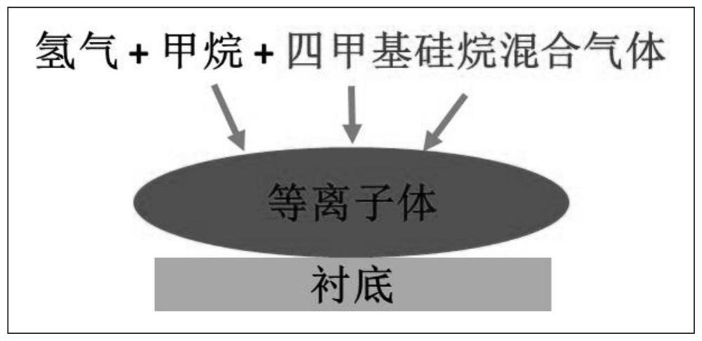
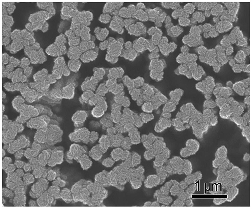
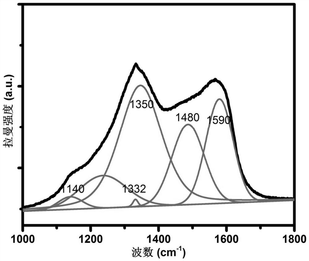
The invention relates to the field of diamond color centers, in particular to a method for preparing high-brightness silicon-vacancy color centers in nano-diamonds. Based on the gas doping method, tetramethylsilane gas is introduced into the microwave plasma chemical vapor deposition equipment to grow silicon-doped nano-diamond film on the substrate. The diamond grain size is less than 100nm, and the substrate is deposited by mechanical stripping or wet etching. The bottom is removed to obtain a self-supporting film and ground to obtain nano-diamond powder. The nano-diamond powder is annealed in an air atmosphere at 550-650 ° C for 5-10 minutes to obtain a silicon vacancy color center whose 738nm fluorescence peak is similar to that of diamond under room temperature excitation conditions. Raman peak intensity ratio is greater than 10. Thus, controllable doping of silicon atoms in nano-diamonds can obtain silicon vacancy color centers, and realize the preparation of silicon vacancy color centers that emit light with high brightness at room temperature. The nano-diamond prepared by the invention has very strong SiV luminescence performance, and can be used in the fields of bioluminescence labeling, high-precision temperature magnetic measurement and the like.
Description
A kind of preparation method of high brightness silicon vacancy color center in nano-diamond technical field The present invention relates to diamond color center field, be specially a kind of high brightness silicon vacancy color center (SiV) in nano-diamond preparation method. Background technique [0002] Diamond is a very important wide band gap semiconductor material, the band gap is 5.45eV, in its device preparation In the process, it is often necessary to add impurity atoms to improve the energy band structure of the semiconductor. Solid solution of specific impurity atoms and crystals in the diamond lattice Lattice-vacancy binding will produce photoluminescence in the visible spectral region, and such combined point defects are called color centers. with polymer Compared with materials such as dye luminescent materials or quantum dots, the radiation fluorescence of diamond color centers has high monochromaticity, no photobleaching, and can be Advantages suc...
Claims
Login to View More Application Information
Patent Timeline
 Patent Type & Authority Patents(China)
IPC IPC(8): C01B32/26C01B32/28
CPCC01B32/26C01B32/28Y02P70/50
Inventor 杨兵姜辛喻彪黄楠刘鲁生
Owner INST OF METAL RESEARCH - CHINESE ACAD OF SCI
- R&D Engineer
- R&D Manager
- IP Professional
- Industry Leading Data Capabilities
- Powerful AI technology
- Patent DNA Extraction
Learn More Browse by: Latest US Patents, China's latest patents, Technical Efficacy Thesaurus, Application Domain, Technology Topic, Popular Technical Reports.
© 2024 PatSnap. All rights reserved.Legal|Privacy policy|Modern Slavery Act Transparency Statement|Sitemap|About US| Contact US: help@patsnap.com


