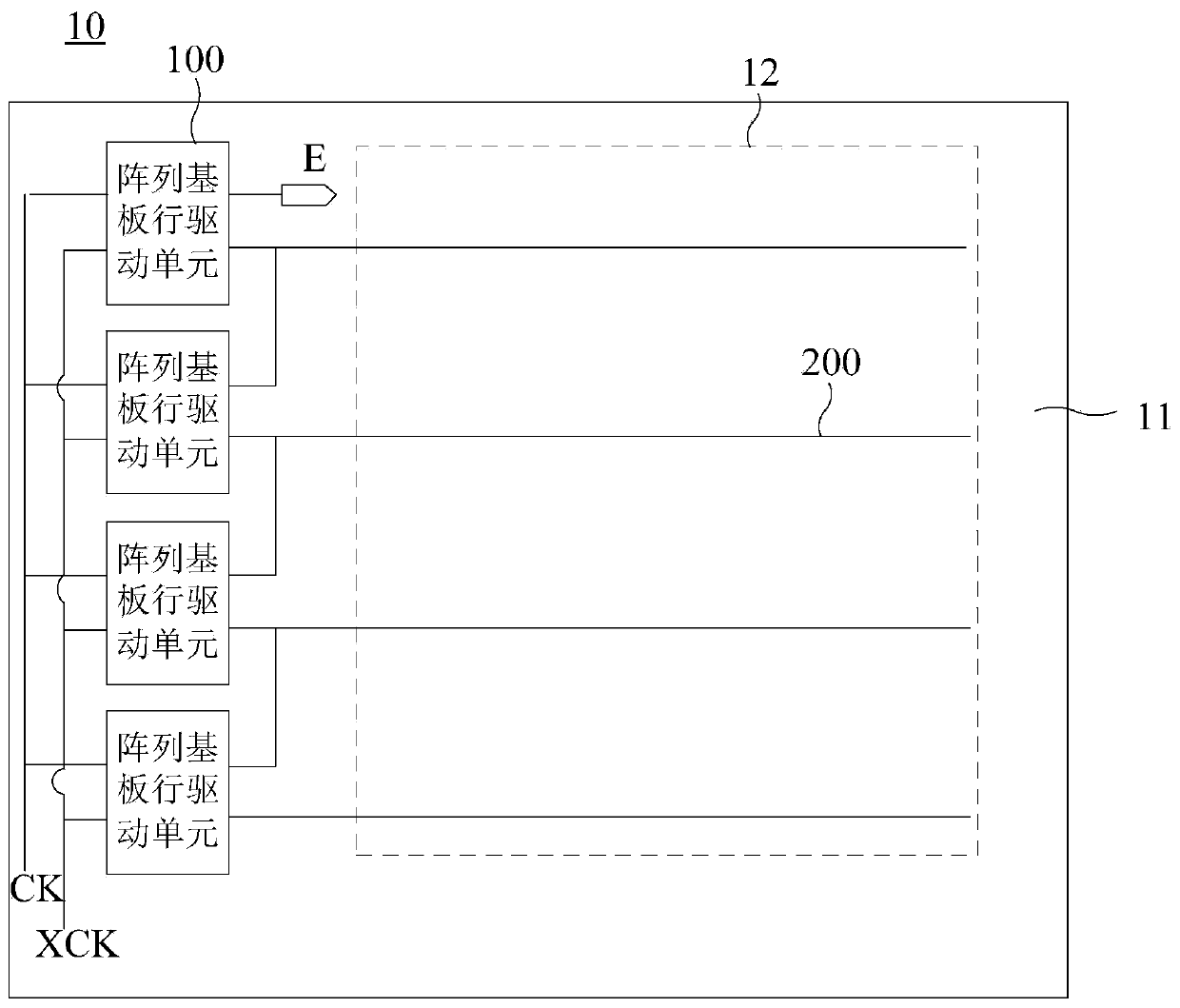
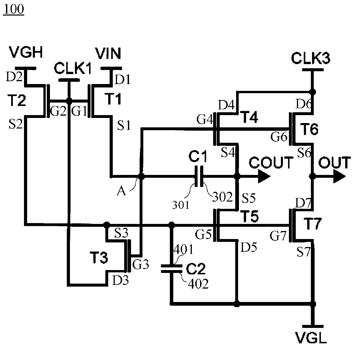
Array substrate row driving circuit and display device
A technology for array substrate rows and driving circuits, which is applied in circuits, electrical components, electrical solid devices, etc., and can solve problems such as threshold voltage drift of thin film transistors
- Summary
- Abstract
- Description
- Claims
- Application Information
AI Technical Summary
Problems solved by technology
Method used
Image
Examples
example 1
[0091] Five thin film transistors with lengths L1, L2, L3, L4, and L5 forming the first lightly doped region and the second lightly doped region respectively have a width-to-length ratio of 10:5 μm, where L1=1.5um, L2=1.0um, L3=0.5um, L4=0.1um, L5=0um. In particular, L5=0um can also correspond to a reference device without an offset feature.
[0092] The specific method of forming the above five thin film transistors is as follows:
[0093] A whole layer of active layer is formed on the base substrate, the main material of the whole layer of active layer is oxide semiconductor, the dopant material is tantalum, and the thickness is 20nm, and then the whole layer of active layer is patterned to obtain the active layer. layer;
[0094] The entire gate insulating layer is formed on the active layer by PECVD process, and the entire gate insulating layer is a single layer of SiO 2Thin film, the thickness is 300nm, the deposition temperature is 230℃, the gas and gas ratio used are...
example 2
[0103] Five thin-film transistors with lengths L6, L7, L8, L9, and L10 forming the first lightly doped region and the second lightly doped region respectively have an aspect ratio of 10:5 μm, where L6=1.5um, L7=1.0um, L8=0.5um, L9=0.1um, L10=0um. In particular, L10=0um can also correspond to a reference device without an offset feature.
[0104] The specific method of forming the above five thin film transistors is as follows:
[0105] A whole layer of active layer is formed on the base substrate, the main material of the whole layer of active layer is oxide semiconductor, the dopant material is praseodymium, and the thickness is 20nm, and then the whole layer of active layer is patterned to obtain the active layer. layer;
[0106] The entire gate insulating layer is formed on the active layer by PECVD process, and the entire gate insulating layer is a single layer of SiO 2 Thin film, the thickness is 300nm, the deposition temperature is 230℃, the gas and gas ratio used are...
example 3
[0115] Five thin film transistors with lengths L11, L12, L13, L14, and L15 forming the first lightly doped region and the second lightly doped region respectively have an aspect ratio of 10:5 μm, where L11=1.5um, L12=1.0um, L13=0.5um, L14=0.1um, L15=0um. In particular, L15=0um can also correspond to a reference device without an offset feature.
[0116] The specific method of forming the above five thin film transistors is as follows:
[0117] The entire active layer is formed on the base substrate, the main material of the entire active layer is oxide semiconductor, the doping material is ytterbium, and the thickness is 30nm, and then the entire active layer is patterned to obtain the active layer. layer;
[0118] The entire gate insulating layer is formed on the active layer by PECVD process, and the entire gate insulating layer is a single layer of SiO 2 Thin film, the thickness is 300nm, the deposition temperature is 250℃, the gas and gas ratio used are SiH 4 / N 2 O / A...
PUM
| Property | Measurement | Unit |
|---|---|---|
| Thickness | aaaaa | aaaaa |
| Thickness | aaaaa | aaaaa |
Abstract
Description
Claims
Application Information
 - R&D
- Intellectual Property
- Life Sciences
- Materials
- Tech Scout
- Unparalleled Data Quality
- Higher Quality Content
- 60% Fewer Hallucinations
Browse by: Latest US Patents, China's latest patents, Technical Efficacy Thesaurus, Application Domain, Technology Topic, Popular Technical Reports.
© 2025 PatSnap. All rights reserved.Legal|Privacy policy|Modern Slavery Act Transparency Statement|Sitemap|About US| Contact US: help@patsnap.com


