Design method of heterogeneous film structure delay line type surface acoustic wave device

A technology of surface acoustic wave devices and thin-film structures, which is applied to electrical components, impedance networks, etc., can solve problems such as difficult device integration, piezoelectric single crystal substrates, difficult semiconductor technology compatibility, and inability to refine infinitely.

Active Publication Date: 2020-04-24
XIAN UNIV OF SCI & TECH
View PDF4 Cites 1 Cited by
  • Summary
  • Abstract
  • Description
  • Claims
  • Application Information

AI Technical Summary

Problems solved by technology

Most of the current surface acoustic wave devices are based on piezoelectric single crystal material substrates. Since the center frequency of surface acoustic wave devices is proportional to the surface acoustic wave velocity of the material, it is inversely proportional to the finger width of the interdigital transducer, and piezoelectric single crystal The surface acoustic wave velocity of the material is determined by the piezoelectric single crystal material, and the wave velocity is determined after the material is selected. Usually, the surface acoustic wave velocity of the piezoelectric single crystal substrate is relatively low, and the width of the fingers is limited by the photolithography process. infinite refinement
Therefore, the piezoelectric single crystal surface acoustic wave device is greatly limited in the high-frequency field, and the piezoelectric single crystal substrate is difficult to be compatible with semiconductor technology, and it is difficult to realize device integration

Method used


Image

  • Design method of heterogeneous film structure delay line type surface acoustic wave device
  • Design method of heterogeneous film structure delay line type surface acoustic wave device

Examples


Embodiment Construction

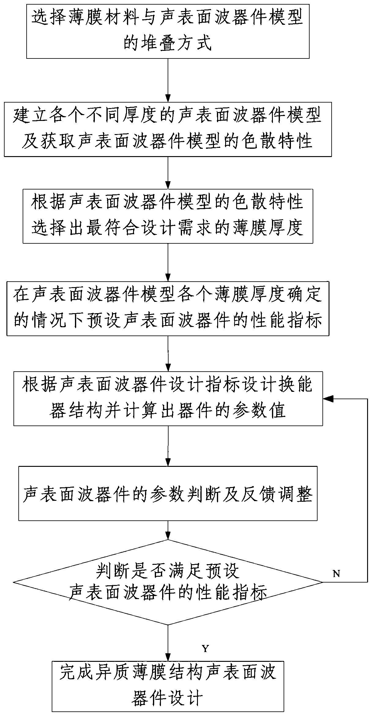
[0052] Such as figure 1 with figure 2 A method for designing a delay-line surface acoustic wave device with a heterogeneous thin-film structure is shown, the method comprising the following steps:

[0053] 1. Select the stacking method of the thin film material and the surface acoustic wave device model:

[0054] Step 101, selecting a sapphire substrate, selecting gallium nitride piezoelectric film and aluminum nitride piezoelectric film, and selecting silicon dioxide as the temperature compensation layer;

[0055] Step 102, setting the bottom-up stacking sequence of the surface acoustic wave device model as sapphire substrate, gallium nitride piezoelectric film, aluminum nitride piezoelectric film layer and temperature compensation layer;

[0056]2. Establish SAW device models with different thicknesses and obtain the dispersion characteristics of SAW device models:

[0057] Step 201, set the wavelength of the surface acoustic wave as λ, and λ=4 μm, and set the thickness ...


PUM

PropertyMeasurementUnit
Frequencyaaaaaaaaaa
Insertion lossaaaaaaaaaa

Abstract

The invention discloses a design method of a heterogeneous thin film structure delay line type surface acoustic wave device. The method comprises the following steps of 1, selecting a stacking mode ofa thin film material and a surface acoustic wave device model; 2, establishing surface acoustic wave device models with different thicknesses and acquiring dispersion characteristics of the surface acoustic wave device models; 3, according to the dispersion characteristic of the surface acoustic wave device model, selecting the film thickness which most meets the design requirement; 4, presettinga performance index of the surface acoustic wave device under the condition that the thickness of each film of the surface acoustic wave device model is determined; 5, designing a transducer structure according to the design indexes of the surface acoustic wave device, and calculating parameter values of the device; and 6, performing parameter judgment and feedback adjustment on the surface acoustic wave device. The method is simple in step, sapphire is selected as a substrate layer, an aluminum nitride and gallium nitride double-layer piezoelectric film is selected, and design of the delay line type surface acoustic wave device of the heterogeneous film structure is achieved.

Description

technical field [0001] The invention belongs to the technical field of surface acoustic wave device design, and in particular relates to a design method of a delay line type surface acoustic wave device with a heterogeneous film structure. Background technique [0002] With the rapid development of electronic information technology, electronic communication equipment continues to develop in the direction of high frequency and miniaturization, which makes discrete components such as internal surface acoustic wave devices continue to develop in the direction of high frequency and integration. Most of the current surface acoustic wave devices are based on piezoelectric single crystal material substrates. Since the center frequency of surface acoustic wave devices is proportional to the surface acoustic wave velocity of the material, it is inversely proportional to the finger width of the interdigital transducer, and piezoelectric single crystal The surface acoustic wave velocit...

Claims


Application Information

Patent Timeline
IPC IPC(8): H03H9/145H03H9/25H03H3/013
CPCH03H9/145H03H9/25H03H3/013
Inventor 张涛柯贤桐王益祎曹晓闯朱寒姜峰
Owner XIAN UNIV OF SCI & TECH
Why Eureka
Try Eureka