Hundred-nanosecond-level trapezoidal wave pulse forming network and design method

A design method and trapezoidal wave technology, applied in pulse shaping, electric pulse generator circuit, calculation, etc., can solve the problems of large heat generation, large damage rate and low life of ceramic capacitors, achieve simple structure, prolong working life, High matching effect

Active Publication Date: 2019-09-27
INST OF APPLIED ELECTRONICS CHINA ACAD OF ENG PHYSICS
View PDF7 Cites 2 Cited by
  • Summary
  • Abstract
  • Description
  • Claims
  • Application Information

AI Technical Summary

Problems solved by technology

For example, "Design and Experimental Research of Pulse Forming Network · Wang Qingfeng · 2009", "Design of Linear Transformer Driving Source Based on Blumlein Pulse Forming Network · Li Mingjia · 2011", "Design of Optical Switch Cascaded Blumlein Type Pulse Network · Ma Xun · 2013", "Solid Pulse Forming Network Marx Pulse Generator · Li Zhiqiang · 2014", but the ceramic capacitor generates a lot of heat, and the lifespan is relatively short when working at a repetition rate under pulse high voltage, and the damage rate is high
[0005] From the above analysis, it can be known that based on the classical theory, if the artificial line network is used to fit the square wave pulse, the network series will not be too low, and once the number of capacitors is large , considering the size, only ceramic capacitors can be used. This kind of network design is not difficult, but the life span is low when the high-voltage repetition frequency works for a long time.

Method used


Image

  • Hundred-nanosecond-level trapezoidal wave pulse forming network and design method
  • Hundred-nanosecond-level trapezoidal wave pulse forming network and design method
  • Hundred-nanosecond-level trapezoidal wave pulse forming network and design method

Examples


Embodiment 1

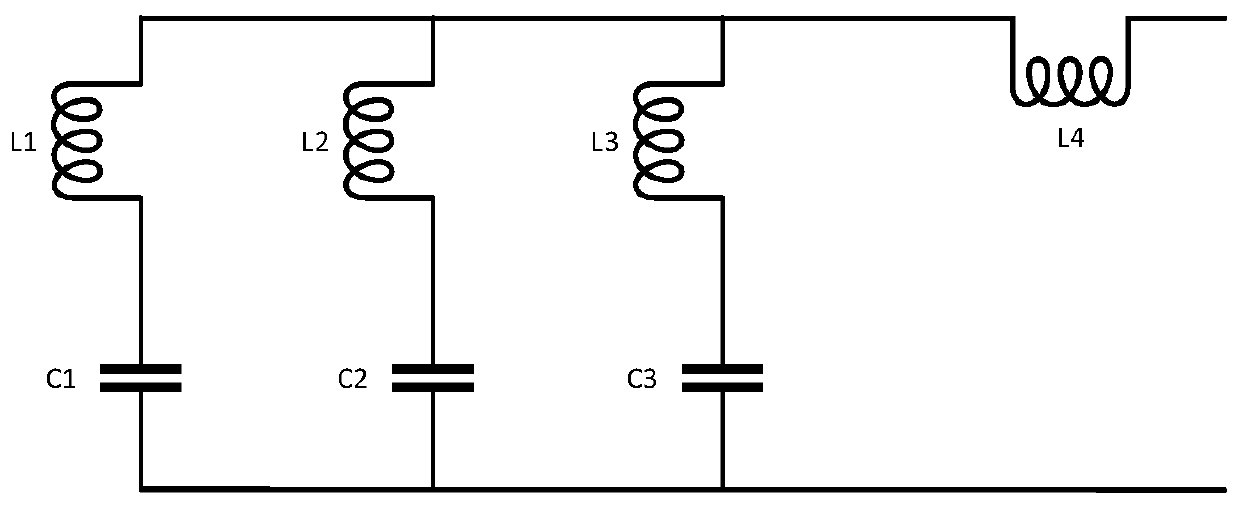
[0049] This embodiment discloses a trapezoidal wave pulse forming network of hundreds of nanoseconds, which includes no more than three LC series branches, wherein the inductance and capacitance of each LC series branch are represented as Ln and Cn respectively, and the not more than After the three LC series branches are connected in parallel, they are connected in series to a shaping inductor L4. The initial values ​​of Ln, Cn, and L4 satisfy the following relationship:

[0050]

[0051]

[0052] n=1, 2..., the upper limit value is the number of LC series branches, a is the initialization parameter, and its value range is between 0.01-0.3, set according to the needs of different application scenarios, ρ is the circuit matching impedance design Value, τ is the design value of the bottom width of the output waveform. Generally, ρ<5Ω, τ<200ns. The value of a is inversely related to the number of network stages (that is, the number of LC series branches in the circuit). ...

Embodiment 2

[0058] This embodiment discloses a method for designing a hundred nanosecond trapezoidal wave pulse forming network, which includes the following steps:

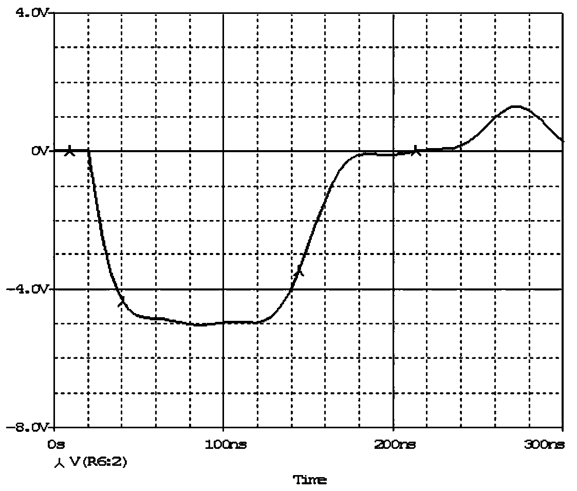
[0059] A. Build a simulation circuit and configure the initial values ​​of each inductor and capacitor. That is, no more than three LC series branches are connected in parallel, and then connected in series with the shaping inductor L4 to complete the construction of the simulation circuit. Configure the initial values ​​of Ln, Cn, and L4 calculated based on formulas (1)-(3) to the corresponding devices. When calculating the initial values ​​of each capacitance and inductance respectively, bit reservation processing is also performed on the settlement results, that is, the calculation results are reserved to ones, tenths, percentiles... . For example, when calculating the initial values ​​of the respective inductances, the calculated values ​​are rounded. Rounding is generally used for rounding. The specific bit reservati...

Embodiment 3

[0066] This embodiment discloses another design method of a hundred nanosecond trapezoidal wave pulse forming network, which includes the following steps:
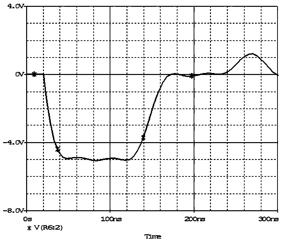
[0067] A. Calculate the initial values ​​of Ln, Cn, and L4 according to formulas (1)-(3), and select the corresponding capacitors and inductors to build the initial circuit. That is, the initial values ​​of Ln, Cn, and L4 are calculated based on formulas (1)-(3), respectively, and the capacitance and inductance of the corresponding values ​​are selected, and Ln and Cn are connected in series to form an LC series branch, and then each series branch is connected in parallel. , in series with L4. When calculating the initial values ​​of each capacitance and inductance respectively, bit reservation processing is also performed on the settlement results, that is, the calculation results are reserved to ones, tenths, percentiles... . For example, when calculating the initial values ​​of the respective inductances, the calculate...


PUM


Abstract

The invention discloses a hundred-nanosecond-level trapezoidal wave pulse forming network and a design method. The network circuit structure comprises a shaping inductor and no more than three LC series branches, and the LC series branches are connected in parallel and then connected to the shaping inductor in series. The capacitor is a pulse film inductor; and capacitance and inductance values are determined through a predetermined method. The design method comprises the steps of building a network circuit structure and determining an initial value of a component, simulating the circuit, and adjusting the parameters of the component according to the output waveform of the circuit. The network structure is simple, the network level is low, the output waveform quality is good, and the research on the high-power microwave technology is facilitated. The design steps are high in operability and wide in application range. The miniaturization of the pulse device can be realized, and the service life of the network is greatly prolonged.

Description

technical field [0001] The invention relates to the technical field of pulse power, in particular to a trapezoidal pulse forming network with a pulse width of hundreds of nanoseconds and a design method thereof. Background technique [0002] Pulse power technology is a technology that stores electrical energy in advance and quickly releases it to the load in a short period of time. It is the basis of high-power microwave technology and has important military and civilian values. Undoubtedly, in order to exert practical value, the miniaturization of the pulse power device must be realized. [0003] In the application of high-power microwaves, pulse power devices are usually required to generate pulse widths on the order of hundreds of nanoseconds, fast rising edges, and wide flat tops, which are ideal square waves. But a complete square wave is difficult to achieve, and a certain degree of trapezoidal wave can be accepted. Conventional pulse power devices use bulky coaxial ...

Claims


Application Information

Patent Timeline
Patent Type & Authority Applications(China)
IPC IPC(8): G06F17/50H03K3/02H03K5/01
CPCH03K3/02H03K5/01G06F30/18
Inventor 张北镇宋法伦甘延青金晓李春霞
Owner INST OF APPLIED ELECTRONICS CHINA ACAD OF ENG PHYSICS
Why Eureka
Try Eureka