


Quick Research
Generate reliable direction feasibility study reports for your R&D in just a few steps.

Technical Q&A
Discover and master advanced knowledge NOW. Basics, ideas, possibilities, all at once.

Find Solutions
As an expert in R&D theories, this can generate solutions to your technical problems instantly.

Evaluate Feasibility
Analyze your overall solution with one click, know your potential R&D risks in advance.

Monitor Landscape
Get weekly tech updates, stay abreast of the latest tech innovations and key insights.
A kind of preparation method of metal substrate
A metal substrate and metal layer technology, applied in semiconductor/solid-state device manufacturing, semiconductor devices, electrical components, etc., can solve problems such as surface roughness of metal substrates and achieve cost-saving effects
- Summary
- Abstract
- Description
- Claims
- Application Information
AI Technical Summary
Problems solved by technology
Method used
Image

Examples
preparation example Construction
[0028] Please refer to Figure 1-Figure 4 , an embodiment of the present invention provides a method for preparing a metal substrate, including:
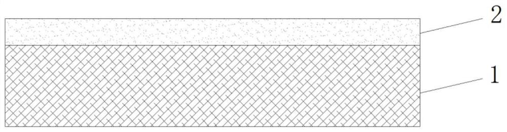
[0029] Disposing a sacrificial layer 2 on the mother board 1 with an atomically smooth surface;
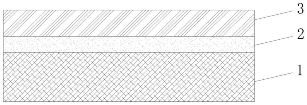
[0030] A metal layer 3 is provided on the side of the sacrificial layer 2 away from the motherboard 1;
[0031] The metal layer 3 is separated from the sacrificial layer 2, and the separated metal layer 3 is the obtained metal substrate.
[0032] The motherboard can be an existing conventional substrate, such as a sapphire substrate, a Si substrate, a GaAs substrate, an InP substrate, a GaP substrate or a quartz substrate. It should be understood that the motherboard is not limited to those listed above. substrate.
[0033] The above-mentioned way of setting the sacrificial layer can use PECVD to grow a layer of SiO2 or SiNx layer, or use evaporation or sputtering equipment to deposit a layer of Ti layer, Al layer, Ni layer, etc., or ...
Embodiment 1
[0049] A preparation method of a metal substrate, comprising the following steps:
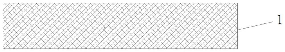
[0050] S11. Provide a motherboard 1 with an atomically smooth upper surface, such as figure 1 shown;
[0051] S12, disposing a sacrificial layer 2 on the upper surface of the motherboard 1, such as figure 2 shown;
[0052] S13, disposing the metal layer 3 of the multi-layer stack structure on the upper surface of the sacrificial layer 2, such as image 3 shown;
[0053] S14, peeling off the metal layer 3 from the sacrificial layer 1 to obtain a metal layer 3 with a smooth surface, and the metal layer 3 obtained by peeling off is the prepared metal substrate, such as Figure 4 shown.
Embodiment 2
[0055] A preparation method of a metal substrate, comprising the following steps:
[0056] S21. Provide a mother board 1 with an atomically smooth surface, adjust the mother board 1 to a target shape and target size, and then make a graphic structure 11 on the upper surface of the mother board 1, such as Figure 5 shown;
[0057] S22, disposing a sacrificial layer 2 on the upper surface of the motherboard 1, such as Image 6 shown;
[0058] S23, disposing a metal layer 3 on the upper surface of the sacrificial layer 2, such as Figure 7 shown;
[0059] S24, peeling off the metal layer 3 from the sacrificial layer 2 to obtain a metal substrate with a smooth surface, the metal substrate having a pattern structure complementary to the pattern structure on the motherboard 1, such as Figure 8 shown.
[0060] In the above embodiments 1 and 2, the selection and setting of the motherboard, the setting of the sacrificial layer, the setting of the metal layer, and the method of se...
PUM
 Abstract
Description
Claims
Application Information
 - R&D Engineer
- R&D Manager
- IP Professional
- Industry Leading Data Capabilities
- Powerful AI technology
- Patent DNA Extraction
Browse by: Latest US Patents, China's latest patents, Technical Efficacy Thesaurus, Application Domain, Technology Topic, Popular Technical Reports.
© 2024 PatSnap. All rights reserved.Legal|Privacy policy|Modern Slavery Act Transparency Statement|Sitemap|About US| Contact US: help@patsnap.com