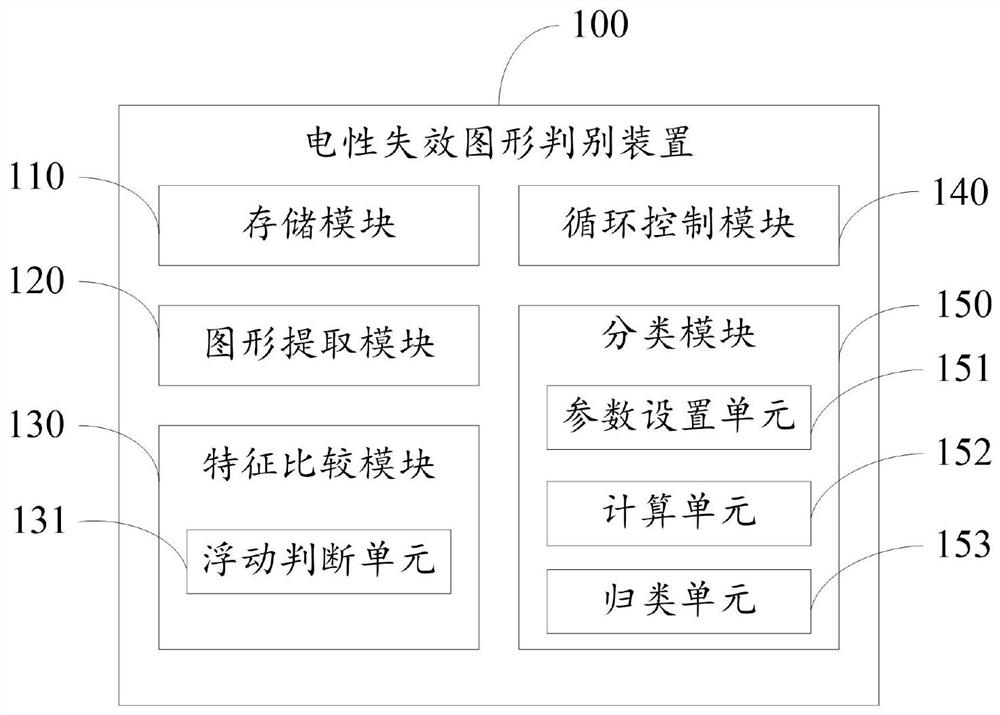
Electrical failure pattern discrimination device and discrimination method
A technology for electrical failure and identification devices, which is applied in the direction of circuit, electrical components, semiconductor/solid-state device testing/measurement, etc., can solve the problem of high loss and achieve the effect of improving accuracy
- Summary
- Abstract
- Description
- Claims
- Application Information
AI Technical Summary
Problems solved by technology
Method used
Image

Examples
Embodiment Construction
[0045] When using electrical failure patterns to analyze the yield rate of chip products such as DRAM chips, the current process of analyzing electrical failure patterns is to select electrical failure patterns randomly or based on stored information (such as storage time, file name, etc.) for pattern feature discrimination And classified to obtain the number of failed chips under different failure categories and perform yield analysis.
[0046] The inventors found that, when discriminating and categorizing the graphic features of multiple electrical failure graphics, if the graphic features of the electrical failure graphics identified later in the sequence include a discriminated and classified electrical failure graphic feature, the electrical failure pattern judged later in the order will be preferentially classified into the same category as the identified and classified electrical failure pattern, but although the pattern features of the electrical failure pattern judged ...
PUM
 Abstract
Description
Claims
Application Information
 - R&D
- Intellectual Property
- Life Sciences
- Materials
- Tech Scout
- Unparalleled Data Quality
- Higher Quality Content
- 60% Fewer Hallucinations
Browse by: Latest US Patents, China's latest patents, Technical Efficacy Thesaurus, Application Domain, Technology Topic, Popular Technical Reports.
© 2025 PatSnap. All rights reserved.Legal|Privacy policy|Modern Slavery Act Transparency Statement|Sitemap|About US| Contact US: help@patsnap.com