
Through hole welding spot for circuit board and circuit board

A circuit board and solder joint technology, applied in the directions of printed circuits, printed circuits, printed circuit components, etc., can solve problems such as difficulty in detecting point information, waste of circuit boards or universal boards, and increase in development costs of semi-finished products. The effect of short circuit or damage to the circuit board

Pending Publication Date: 2020-02-07
中昊芯英(杭州)科技有限公司
View PDF0 Cites 0 Cited by
  • Summary
  • Abstract
  • Description
  • Claims
  • Application Information

AI Technical Summary

Problems solved by technology

However, the first technical solution will cause waste of use of circuit boards or universal boards, and it is not easy to record the information of detection points conveniently and accurately; the second technical solution will increase unnecessary development costs of semi-finished products

Method used


Image

  • Through hole welding spot for circuit board and circuit board
  • Through hole welding spot for circuit board and circuit board
  • Through hole welding spot for circuit board and circuit board

Examples


Embodiment Construction

[0023] The following will clearly and completely describe the technical solutions in the embodiments of the present invention with reference to the accompanying drawings in the embodiments of the present invention. Obviously, the described embodiments are only some, not all, embodiments of the present invention. Based on the embodiments of the present invention, all other embodiments obtained by persons of ordinary skill in the art without creative efforts fall within the protection scope of the present invention.

[0024] It should be noted that when an element is referred to as being “fixed” or “disposed on” another element, it may be directly on the other element or be indirectly on the other element. When an element is referred to as being "connected to" another element, it can be directly connected to the other element or indirectly connected to the other element.

[0025] It should be understood that the terms "row direction", "column direction", "top", "bottom", "front"...


PUM


Abstract

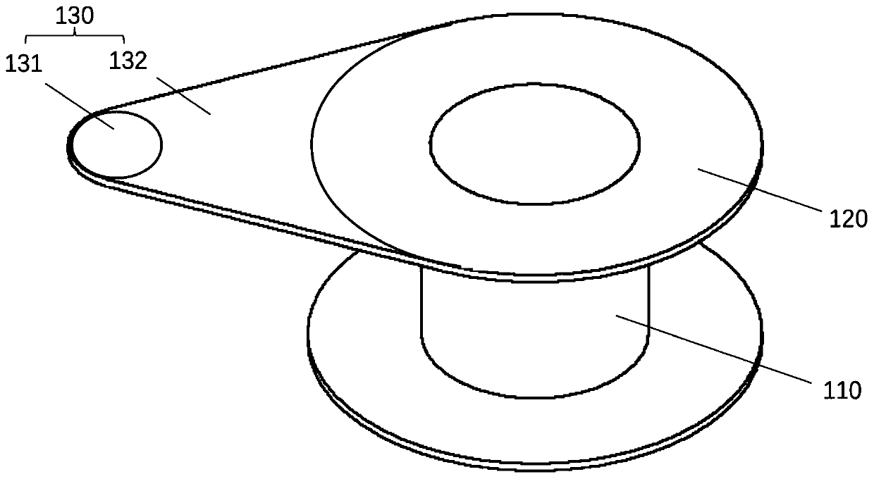
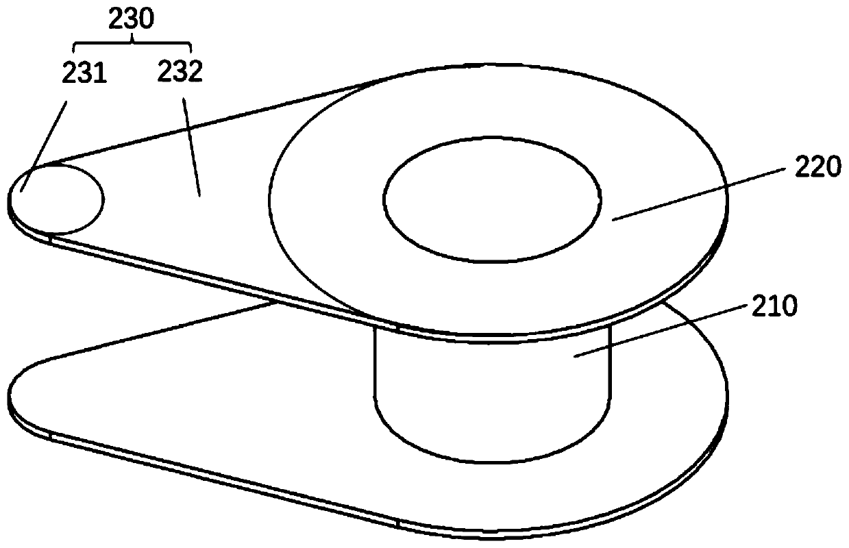
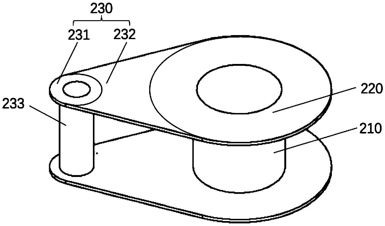
The invention discloses a through hole welding spot for a circuit board and is particularly suitable for a universal board with frequent detection requirements and higher flexibility requirements. Thethrough hole welding spot comprises a bonding pad, an auxiliary welding area and a transition area arranged between the bonding pad and the auxiliary welding area, and an anti-welding ink layer is arranged on a surface of the transition area. The auxiliary welding area is utilized as a detection point, so detection of the circuit board is more convenient and faster, and physical influence of detection operation on welding spots can be avoided; under the condition that the circuit board manufacturing process and the circuit element welding technology are not changed, debugging difficulty of the circuit board in the development process is greatly reduced, and the development process of the circuit board is accelerated.

Description

technical field [0001] The invention relates to the technical field of integrated circuits, in particular to through-hole solder joints for circuit boards. Background technique [0002] With the continuous increase of the types of printed circuit components, the continuous reduction of the size of the components and the continuous increase of the complexity of the circuit board, the development of the printed circuit board, especially in the process of sample development using the universal board (Universal Board), due to the complex Components and circuit wiring, it becomes more and more difficult to use a multimeter for circuit error correction. The unevenness of the solder joints makes the positioning of the multimeter pen needle difficult and easy to slip, and the surface oxide layer of the solder joints makes the measurement unstable and unreliable. Especially in some sensitive areas, the slippage of the multimeter pen needle may cause damage to the circuit board or ev...

Claims


Application Information

Patent Timeline
Patent Type & Authority Applications(China)
IPC IPC(8): H05K1/11
CPCH05K1/116H05K2201/09481
Inventor 王博赟杨龚轶凡郑瀚寻闯小明
Owner 中昊芯英(杭州)科技有限公司
Learn More