Process method for truncating polysilicon gate of fin transistor

A fin transistor and polysilicon gate technology, which is applied in the field of polysilicon gate truncation, can solve the problems of reducing product yield, polysilicon etching residue, polysilicon removal, etc., and achieves the effects of improving product yield, improving process window, and preventing polysilicon residues.

Active Publication Date: 2020-02-04
SHANGHAI HUALI INTEGRATED CIRCUTE MFG CO LTD
View PDF11 Cites 2 Cited by
  • Summary
  • Abstract
  • Description
  • Claims
  • Application Information

AI Technical Summary

Problems solved by technology

[0014] Depend on Figure 1B It can be seen that the depth of polysilicon etching is relatively deep, and as the height of the polysilicon gate 106 increases, the depth of polysilicon etching will increase, which will make the polysilicon etching have a larger aspect ratio, Increased etching difficulty makes it easy to form polysilicon etching residues. For example, the polysilicon cannot be completely removed in the bottom area of ​​the groove formed by etching, that is, the area indicated by the dotted circle corresponding to the mark 108, which may cause short circuits in subsequent components. Reduce product yield

Method used


Image

  • Process method for truncating polysilicon gate of fin transistor
  • Process method for truncating polysilicon gate of fin transistor
  • Process method for truncating polysilicon gate of fin transistor

Examples


Embodiment Construction

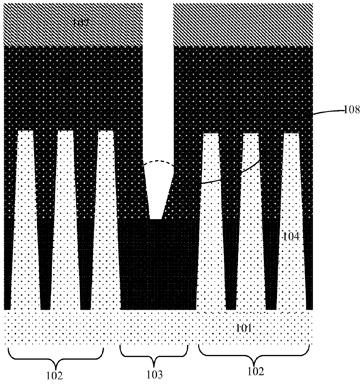
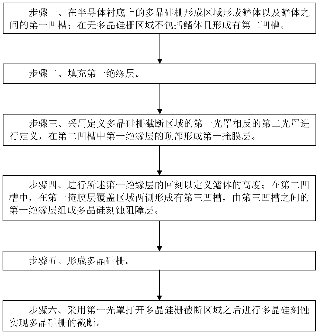
[0049] Such as figure 2 As shown, it is a flow chart of the process method of polysilicon gate truncation of the fin transistor of the embodiment of the present invention; as Figure 3A to Figure 3F As shown, it is a schematic diagram of the device structure in each step of the process method of polysilicon gate truncation of fin transistor in the embodiment of the present invention; the process method of polysilicon gate truncation of fin transistor in the embodiment of the present invention includes the following steps:

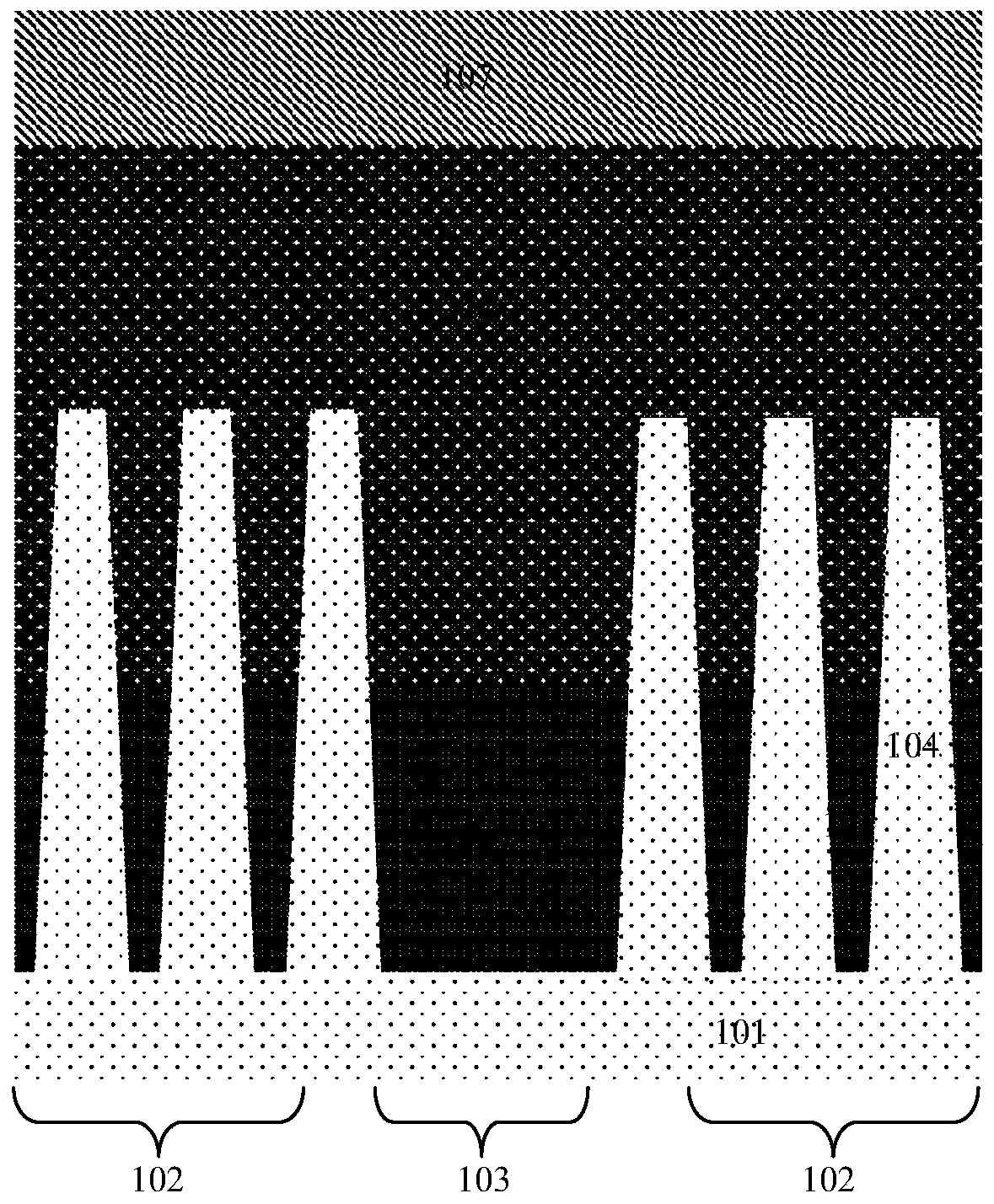
[0050] Step 1, such as Figure 3A As shown, a semiconductor substrate 1 is provided, and the semiconductor substrate 1 includes a polysilicon gate forming region 201 and a polysilicon gate-free region 202 .

[0051] A plurality of fin bodies 2 formed by etching the semiconductor substrate 1 are formed in the polysilicon gate formation region 201 , and first grooves 3 are formed between each of the fin bodies 2 . Each of the fins 2 is strip-shaped and paral...


PUM


Abstract

The invention discloses a process method for truncating a polysilicon gate of a fin transistor. The process method comprises the following steps of step 1, forming fin bodies and a first groove between the fin bodies in a polysilicon gate formation region on a semiconductor substrate, and the fin bodies are not included in a polysilicon-free gate region and a second groove is formed; step 2, filling a first insulating layer; step 3, using a second photomask opposite to a first photomask that defines a polysilicon gate truncated region to define, and forming a first mask layer at the top of thefirst insulating layer in the second groove; step 4, etching back the first insulating layer, so as to define the height of the fin bodies; in the second groove, forming third grooves at the two sides of a coverage region of the first mask layer, and forming a polysilicon etching barrier layer by the first insulating layer between the third grooves; step 5, forming the polysilicon gate; and step6, after the polysilicon gate truncated region is opened by the first mask, performing polysilicon etching to achieve the truncation of the polysilicon gate. The process method for truncating the polysilicon gate of the fin transistor provided by the invention can increase process windows and improve the product yield.

Description

technical field [0001] The invention relates to the field of semiconductor integrated circuit manufacturing, in particular to a polysilicon gate cut-off process method for a fin transistor (FinFET transistor). Background technique [0002] In the existing Fin-type transistor logic chip process, the height of the polysilicon gate needs to be increased to meet the requirements of subsequent processes. The increase in the height of the polysilicon gate will cause insufficient window when the polysilicon gate is cut off in the process flow, which may cause short circuit problems in subsequent components. Such as Figure 1A to Figure 1B Shown is a schematic diagram of the device structure in each step of the polysilicon gate truncation process of the existing fin transistor; the polysilicon gate truncation process of the existing fin transistor includes the following steps: [0003] Step 1, such as Figure 1A As shown, a semiconductor substrate 101 is provided, and the semicondu...

Claims


Application Information

Patent Timeline
Patent Type & Authority Applications(China)
IPC IPC(8): H01L21/28H01L21/336
CPCH01L21/28035H01L29/66795H01L21/823431H01L21/823437H01L21/76229H01L21/823481H01L27/0886H01L29/7851
Inventor 李镇全陈颖儒刘立尧胡展源
Owner SHANGHAI HUALI INTEGRATED CIRCUTE MFG CO LTD
Why Eureka
Try Eureka