Composite high-frequency substrate with characteristics of high Dk and low Df and preparation method thereof
A composite and characteristic technology, applied in the direction of circuit substrate materials, printed circuit components, electrical components, etc., can solve the problems that cannot really meet high frequency and high speed, cannot meet high Dk requirements, and is prone to high leakage current, etc., to achieve excellent Thermal stability, good electrical properties, good electrical properties
- Summary
- Abstract
- Description
- Claims
- Application Information
AI Technical Summary
Problems solved by technology
Method used
Image
Examples
Embodiment approach
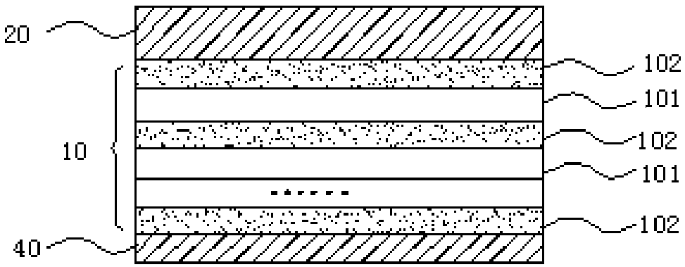
[0062] Embodiment: A composite high-frequency substrate with high Dk and low Df characteristics, such as Figure 1 to Figure 4 As shown, it includes a first copper foil layer 20 and a core layer 10. The core layer 10 includes several polymer film layers 101 and several dielectric adhesive layers, and the adjacent polymer film layers are laminated with the dielectric adhesive Together, the first copper foil layer is located on the surface of the outermost dielectric adhesive layer of the core layer, and the dielectric adhesive layer includes at least one of the first dielectric adhesive layer 102 and the second dielectric adhesive layer 103 One, the first dielectric adhesive layer refers to an adhesive layer with a Dk value of 6-30 (10G HZ) and a Df value of 0.002-0.020 (10G HZ), and the second dielectric adhesive layer refers to a Dk value of 15- 100 (10G HZ) and an adhesive layer with a Df value of 0.002-0.020 (10G HZ), and the Dk value of the second dielectric adhesive layer...
Embodiment approach 1
[0090] Embodiment 1: A composite high-frequency substrate with high Dk and low Df characteristics, such as figure 1 As shown, the high-frequency substrate is a single-sided adhesive copper-clad substrate, the dielectric adhesive layer is the first dielectric adhesive layer 102, and the core layer 10 is composed of several first dielectric adhesive layers 102 Composed of several polymer film layers 101, the first dielectric adhesive layer is spaced apart from the polymer film layer, and the first dielectric adhesive layer is located on the outermost side of the core layer .
[0091] The single-sided adhesive copper-clad substrate further includes a release layer 30, and the core layer is located between the first copper foil layer and the release layer.
Embodiment approach 2
[0092] Embodiment 2: A composite high-frequency substrate with high Dk and low Df characteristics, such as figure 2 As shown, the structure is similar to Embodiment 1, except that: the high-frequency substrate is a double-sided copper-clad substrate, and the double-sided copper-clad substrate also includes a second copper foil layer 40, and the core layer is located on the Between the first copper foil layer 20 and the second copper foil layer 40 .
PUM
| Property | Measurement | Unit |
|---|---|---|
| thickness | aaaaa | aaaaa |
| thickness | aaaaa | aaaaa |
| thickness | aaaaa | aaaaa |
Abstract
Description
Claims
Application Information
 - R&D
- Intellectual Property
- Life Sciences
- Materials
- Tech Scout
- Unparalleled Data Quality
- Higher Quality Content
- 60% Fewer Hallucinations
Browse by: Latest US Patents, China's latest patents, Technical Efficacy Thesaurus, Application Domain, Technology Topic, Popular Technical Reports.
© 2025 PatSnap. All rights reserved.Legal|Privacy policy|Modern Slavery Act Transparency Statement|Sitemap|About US| Contact US: help@patsnap.com


