
Terahertz semiconductor laser, its preparation method and application

A semiconductor and laser technology, applied in the structure of semiconductor lasers, lasers, optical waveguide semiconductors, etc., can solve the problems of high peak power of single cavity surface, low device power, and high threshold current density, and achieve small beam divergence angle and output power. Improve the effect of simple production process

Active Publication Date: 2020-08-25
INST OF SEMICONDUCTORS - CHINESE ACAD OF SCI
View PDF5 Cites 0 Cited by
  • Summary
  • Abstract
  • Description
  • Claims
  • Application Information

AI Technical Summary

Problems solved by technology

In order to improve the beam quality of the device while increasing the output power of the device, tree array QCL, photonic crystal (Photonic Crystal, PC) QCL, master oscillator power amplifier (Master-oscillator Power-amplifier, MOPA) QCL and oblique New devices such as cavity QCL, in which the tree-shaped array quantum cascade laser composed of Y-shaped units is output in the same phase mode, realizing a single lobe in the far field, but the device power is low and the threshold current density is high
In addition, regarding the production of PC DFB (photonic crystal distributed feedback) quantum cascade lasers, the peak power of the single-cavity surface of the device is relatively high, and the far-field divergence angle near the diffraction limit is obtained, but due to the existence of multiple band-edge modes in the photonic crystal , the device is a dual longitudinal mode laser

Method used


Image

  • Terahertz semiconductor laser, its preparation method and application
  • Terahertz semiconductor laser, its preparation method and application
  • Terahertz semiconductor laser, its preparation method and application

Examples


preparation example Construction

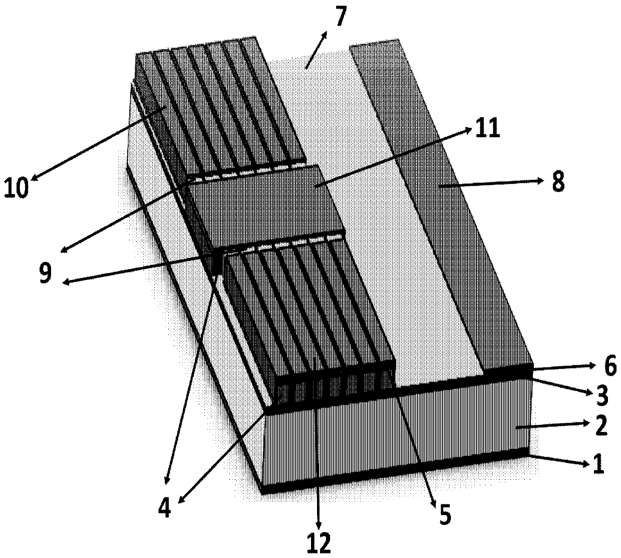
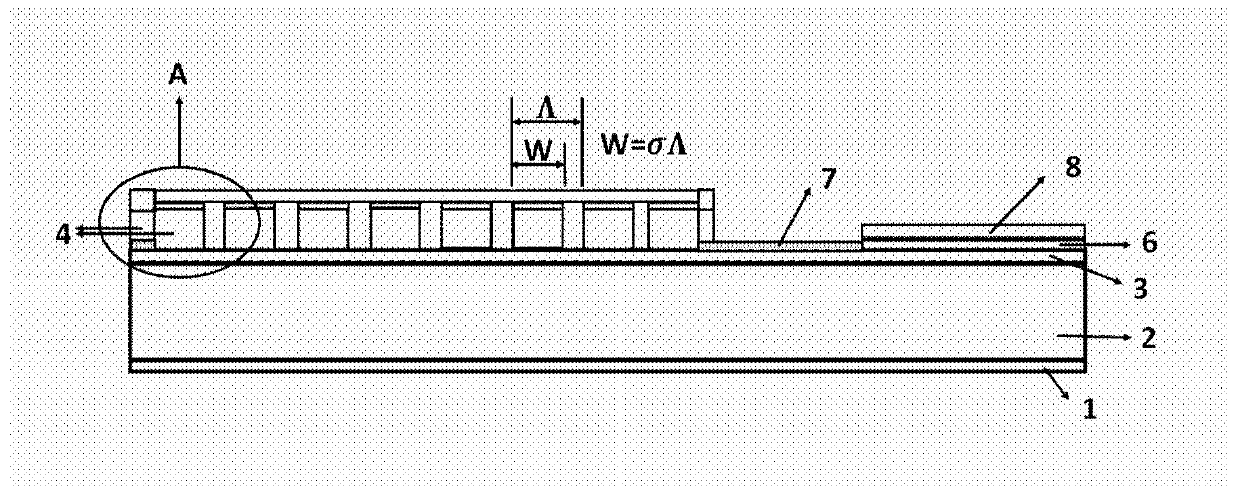
[0075] The present invention also discloses a preparation method of the above-mentioned terahertz semiconductor laser, comprising the following steps:

[0076] (1) sequentially growing a first highly doped layer, an active region, and a second highly doped layer on a supporting substrate;

[0077] (2) Make the first multi-ridge region, the rectangular cavity region, and the second multi-ridge region on the active region and the second highly doped layer, and at the junction of the first multi-ridge region, the second multi-ridge region and the rectangular cavity region Making electrical isolation trenches;

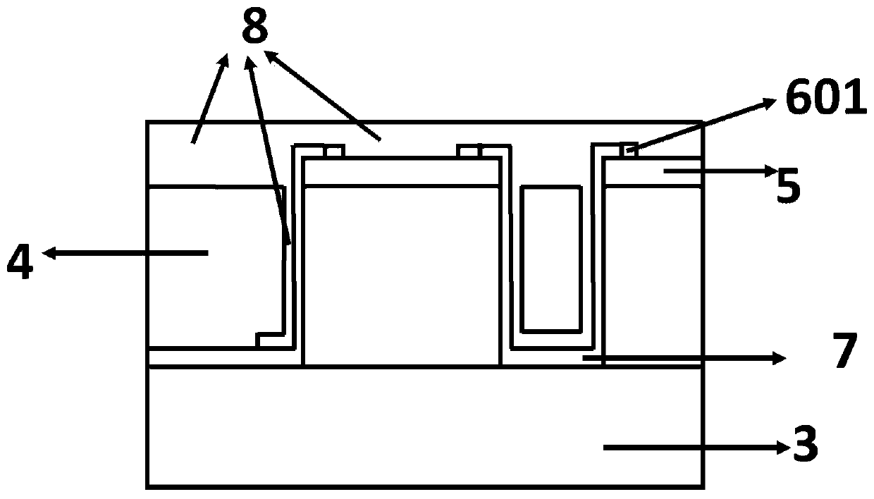
[0078] (3) growing a silicon dioxide layer on the upper surface of the device formed in step (2), and opening an electrical injection window on the silicon dioxide layer;

[0079] (4) making ohmic contact layers respectively on the second highly doped layer and the first highly doped layer of the electrical injection window;

[0080] (5) growing a second metal layer on t...


PUM

PropertyMeasurementUnit
thicknessaaaaaaaaaa
thicknessaaaaaaaaaa

Abstract

The invention provides a terahertz semiconductor laser device and a preparation method thereof and an application thereof. The terahertz semiconductor laser device comprises a first metal layer, a pressure welding metal layer serving as the bottom of the semiconductor laser device and a heat dissipation channel, a supporting substrate, a first highly-doped layer which is arranged on the supportingsubstrate and serves as a lower waveguide light limiting layer of the laser device, an active region growing on the first highly doped layer, a second highly-doped layer positioned on the active region, a plurality of electrical isolation trenches, an ohmic contact layer, an electrical isolation layer and a second metal layer. The terahertz semiconductor laser device is advantaged in that a periodic multi-ridge array and rectangular cavity coupling structure is adopted, and the beam divergence angle in the ridge width direction of the device is improved by means of the self-imaging effect caused by in-phase interference, by using a periodic multi-ridge array, the gain volume of the laser device is increased, and the output power is improved.

Description

technical field [0001] The invention relates to the field of optical waveguide technology of terahertz band semiconductor laser devices, in particular to a terahertz semiconductor laser, its preparation method and application. Background technique [0002] Since the energy value of electromagnetic waves in the terahertz band (0.3-10THz) corresponds to the rotation and vibration energy of some special gas molecules and water molecules, it has unique application value in gas composition detection, medical diagnosis, dangerous goods telemetry, free space communication, etc. Terahertz quantum cascade laser (Quantum Cascade Laser, QCL) is a unipolar terahertz semiconductor laser based on coupled multi-quantum well conduction band sublevel stimulated emission luminescence, which has the characteristics of miniaturization, portability and high continuous power. , has gradually become an ideal terahertz coherent light source for the above applications, so it is of great significance...

Claims


Application Information

Patent Timeline
Patent Type & Authority Patents(China)
IPC IPC(8): H01S5/22H01S5/10
CPCH01S5/1042H01S5/22H01S2304/00
Inventor 赵方圆刘俊岐刘峰奇张锦川翟慎强卓宁王利军刘舒曼王占国
Owner INST OF SEMICONDUCTORS - CHINESE ACAD OF SCI
Learn More