Method for preparing test sample by fib and test sample

A technology for testing samples and samples, applied in the field of preparing test samples by using FIB, can solve the problems of difficulty in obtaining EBSD test samples that meet the requirements, affecting the Bragg diffraction Kikuchi pattern of crystal planes, affecting the accuracy of test results, etc., and reducing the deformation trend. , avoid deformation, reduce the effect of adjustment requirements

Active Publication Date: 2022-04-12
YANGTZE MEMORY TECH CO LTD
View PDF11 Cites 0 Cited by
  • Summary
  • Abstract
  • Description
  • Claims
  • Application Information

AI Technical Summary

Problems solved by technology

[0004] When preparing samples by FIB, some film layers to be tested will be deformed due to internal stress after being thinned due to the deposition process, material properties, etc., and accurate measurement cannot be performed accurately
[0005] For example, when it is necessary to perform EBSD test on the target material layer, the sample of the target material layer prepared by FIB will be deformed, which will seriously affect the Bragg diffraction of the crystal plane and the generation of Kikuchi patterns, thereby affecting the accuracy of the test results
Further, for the EBSD test, the effective area of ​​the sample needs to be larger, such as greater than 9um 2 , while using the existing FIB preparation technology, the larger the effective area of ​​the sample, the easier it is to deform, so it is difficult to obtain an EBSD test sample that meets the requirements

Method used


Image

  • Method for preparing test sample by fib and test sample
  • Method for preparing test sample by fib and test sample
  • Method for preparing test sample by fib and test sample

Examples


Embodiment Construction

[0024] The method for preparing a test sample by using FIB provided by the present invention and the specific implementation of the test sample will be described in detail below in conjunction with the accompanying drawings.

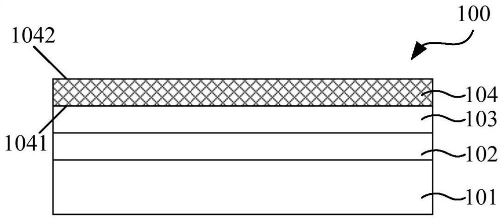
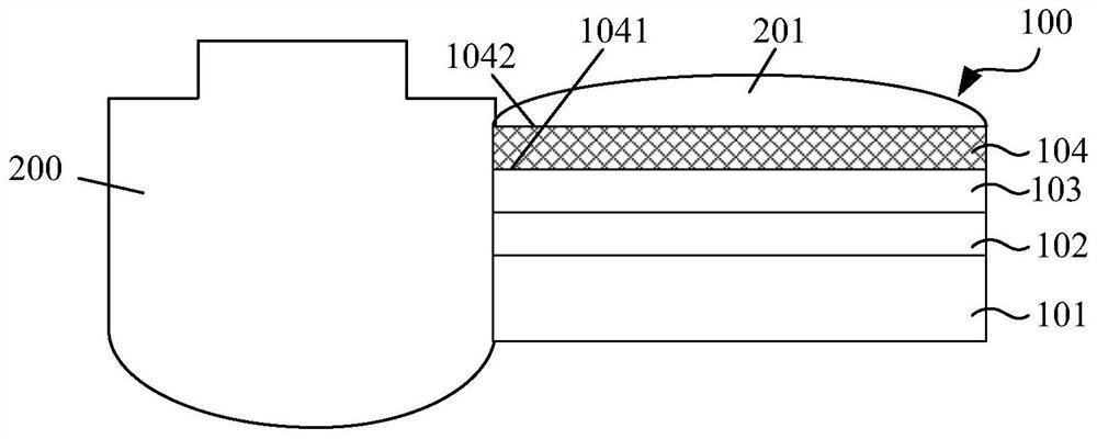
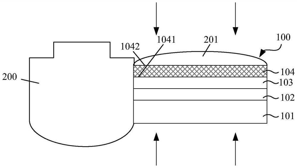
[0025] Please refer to figure 1 , providing a pretreated sample 100 having a target layer 104 having opposing first surfaces 1041 and second surfaces 1042 .

[0026] In this specific embodiment, the pretreatment sample is a pretreatment sample taken from the unstructured wafer (Blanket Wafer) used for adjusting the process adjustment of 3D NAND products by focusing ion beam (FIB).

[0027] The pretreated sample 100 includes: a single crystal silicon layer 101 , a silicon oxide layer 102 , a Ta layer and a target layer 104 , and the target layer 104 is a copper seed layer. In this specific embodiment, the copper seed layer is used as the target layer 104, and the target layer 104 is thinned to a target thickness as a sample for T-EBSD testing. In this ...


PUM

PropertyMeasurementUnit
diameteraaaaaaaaaa
thicknessaaaaaaaaaa
thicknessaaaaaaaaaa

Abstract

The present invention relates to a method for preparing a test sample using FIB and a test sample, the method comprising: providing a pretreated sample with a target layer having opposite first and second surfaces; The pretreated sample is fixed on the sample stage; along the direction towards the first surface and / or the second surface of the target layer, the ion beam is used to perform the first thinning of the pretreated sample, and the thickness of the pretreated sample is reduced. Thinning to a preset thickness; forming several through holes through the pretreated sample; continuing to perform a second thinning on the pretreated sample formed with the through holes until the target layer is thinned to a target thickness. The above method can avoid deformation of the target layer during the thinning process.

Description

technical field [0001] The invention relates to the technical field of semiconductors, in particular to a method for preparing test samples by using FIB. Background technique [0002] The use of focused ion beam (FIB) has become an important method for special sample preparation and fine structure processing because of its high precision and fast sample preparation. It is widely used in the preparation of TEM (projection electron microscope), SEM (scanning electron microscope) and EBSD ( Electron backscattered diffraction electron microscope) test samples. [0003] During the adjustment process of the chip process, it is often necessary to study the growth conditions, microstructure, inter-film bonding force and other properties of each film layer, so as to provide data reference and support for the preparation of structural samples. [0004] When preparing samples by FIB, some film layers to be tested will be deformed due to internal stress after being thinned due to the d...

Claims


Application Information

Patent Timeline
Patent Type & Authority Patents(China)
IPC IPC(8): G01N1/28G01N23/2202G01N23/2005
CPCG01N1/28G01N23/2202G01N23/2005
Inventor 刘婧周阳
Owner YANGTZE MEMORY TECH CO LTD
Why Eureka
Try Eureka