A light-curing 3D printing device
A 3D printing and light curing technology, applied in the field of 3D printing, can solve problems such as increasing printing speed, affecting printing speed and accuracy, and long printing material inflow path, so as to simplify positioning and installation, improve vibration resistance, and reduce bonding area effect
- Summary
- Abstract
- Description
- Claims
- Application Information
AI Technical Summary
Problems solved by technology
Method used
Image
Examples
Embodiment 1
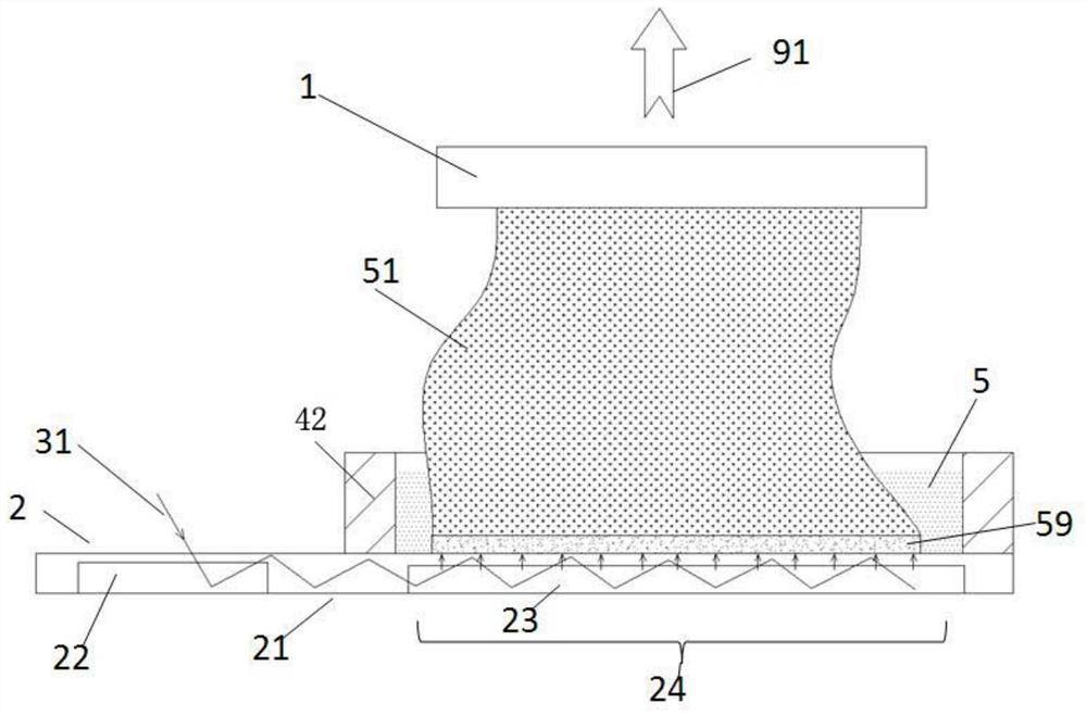
[0048] Such as figure 1 A light-curing 3D printing device shown includes a model board 1 and a light guide assembly 2 , and a curing model 51 is combined on the model board 1 . The light guide assembly 2 includes an optical waveguide 21 , an in-coupling portion 22 and an out-coupling portion 23 , and a region of the light guide assembly 2 corresponding to the out-coupling portion 23 is an out-coupling region 24 . The outcoupling area 24 of the light guide assembly 2 is set corresponding to the model plate 1, and the distance between the model plate 1 and the light guide assembly 2 can be controlled and adjusted, that is, the relative movement between the model plate 1 and the light guide assembly 2 can be carried out, such as The template plate 1 moves away from the light guide assembly 2 in the direction of the arrow 91 , or the light guide assembly 2 moves away from the template plate 1 . The relative movement between the model plate 1 and the light guide assembly 2 can als...
Embodiment 2
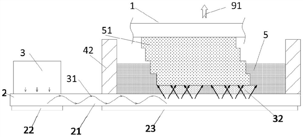
[0053] Such as figure 2 As shown, the light beam 31 emitted by the light source 3 shoots to the coupling part 22, and the coupling part 22 adjusts the direction of the light beam 31 and injects it into the optical waveguide 21. The figure shows that the light beam 31 propagates in the form of a sine wave in the optical waveguide 21 and reaches the outcoupling part 23. The outcoupling unit 23 adjusts the direction of the light beam 31 and emits it toward the light-transmitting plate 25 to irradiate the printing material 5 for photocuring. In the figure, the in-coupling part 22 and the out-coupling part 23 are externally placed on the outer surface of the optical waveguide 21, such as using gratings, of course, they can also be integrated inside the optical waveguide 21, such as mirrors or semi-transparent mirrors.
[0054] The difference between this embodiment and Embodiment 1 is that the outcoupling part 23 converts the light beam 31 in the outcoupling region 24 of the light...
Embodiment 3
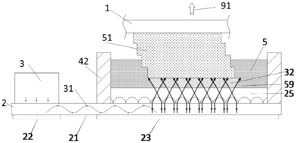
[0056] Such as image 3 As shown, the difference between this embodiment and Embodiment 1 is that a light-transmitting plate 25 is correspondingly provided between the outcoupling area 24 of the light guide assembly 2 and the model plate 1 . A microlens array 26 can also be provided inside the light-transmitting plate 25. After the light beam 31 emitted by the outcoupling unit 23 is transformed (such as focusing) by the micro-lens array 26 of the light-transmitting plate 25, it is directed from the light-transmitting plate 25 toward the model plate. The surface of 1 discretely emits, such as spaced, diffused emission, and forms several beam families 32 between the curing model 51 and the transparent plate 25, and at least part of adjacent beam families 32 may contact or partially overlap. The microlens array 26 can be a variable refractive index microlens array (as shown in the figure) embedded in the light-transmitting plate 25, or can be formed by a semi-convex lens array or...
PUM
 Abstract
Description
Claims
Application Information
 - R&D
- Intellectual Property
- Life Sciences
- Materials
- Tech Scout
- Unparalleled Data Quality
- Higher Quality Content
- 60% Fewer Hallucinations
Browse by: Latest US Patents, China's latest patents, Technical Efficacy Thesaurus, Application Domain, Technology Topic, Popular Technical Reports.
© 2025 PatSnap. All rights reserved.Legal|Privacy policy|Modern Slavery Act Transparency Statement|Sitemap|About US| Contact US: help@patsnap.com


