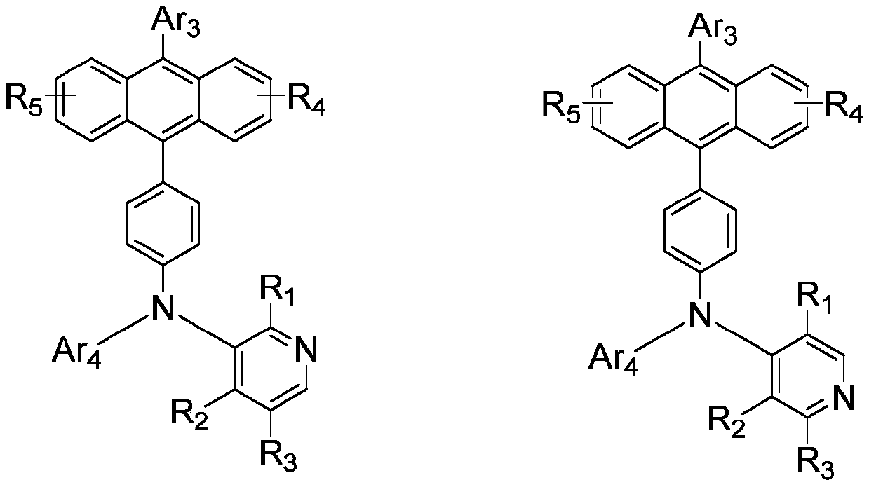
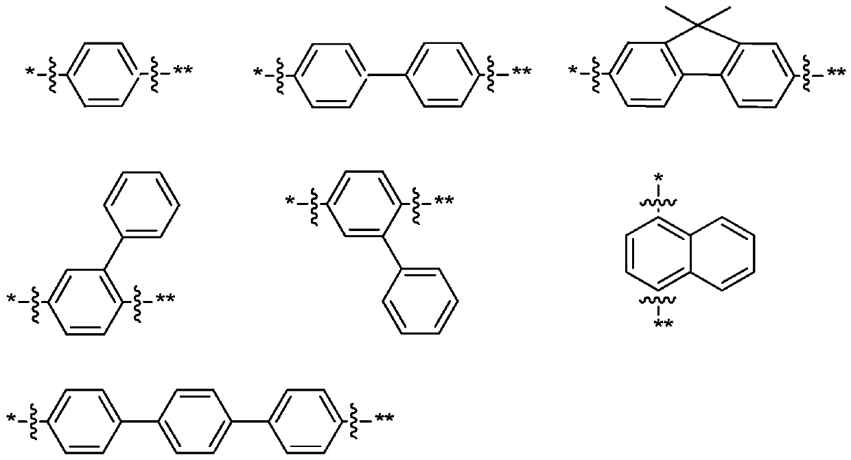
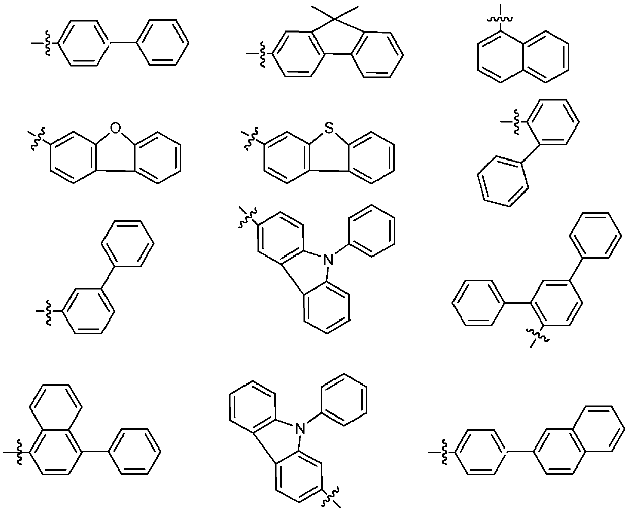
Organic electroluminescent device and electronic apparatus
An electroluminescent device, an organic technology, applied in the direction of electric solid-state devices, electrical components, semiconductor devices, etc., can solve the problems of short lifespan and low luminous efficiency of devices, and achieve improved luminous efficiency, lowered injection barrier, and improved lifespan Effect
- Summary
- Abstract
- Description
- Claims
- Application Information
AI Technical Summary
Problems solved by technology
Method used
Image
Examples
preparation example Construction
[0062] Preparation of compound 1-1
[0063]
[0064] Under the protection of nitrogen, add 133.75mmol of 1-adamantanol, 127.38mmol of 4-chloro-p-terphenyl, and 337mL of dichloromethane into the reaction flask. Concentrated sulfuric acid 318.45mmol. After the dropwise addition was completed, the reaction was kept for 3 hours, and quenched by adding water. Separation, extraction, washing, drying, filtering and concentration. Use a mixed solvent of dichloromethane and n-heptane to pass through the column and recrystallize to a purity (LC)>95%. After drying, white solid 1-(4"-chloro-[1,1':4',1"-terphenyl]-4-yl)adamantane was obtained. Yield: 68%.
[0065]
[0066] Under nitrogen protection, (1,3s)-1-(4"-chloro-[1,1':4',1"-terphenyl]-4-yl)adamantane 86.618mmol was added to the reaction flask, 2 -Amino-9,9-dimethylfluorene 86.618mmol, toluene 691mL, sodium tert-butoxide 259.854mmol, stirring, heating to 70-80°C, slowly adding Pd 2 dba 3 0.86618mmol, s-PHOS 1.7324mmol, ...
Embodiment 1
[0244] Example 1: Fabrication of a blue organic light-emitting device
[0245] A 40mm×40mm×0.7mm thick glass substrate with an ITO transparent electrode (anode) was used for UV ozone and N 2 The coated surface of the substrate is treated with plasma, and then the cleaned anode glass with ITO transparent electrode is placed on the substrate shelf of the vacuum evaporation equipment.
[0246] First, a layer of hexacyanine-1,4,5,8,9,11-hexaazatriphenylene-hexacarbonitrile (HAT-CN) film with a thickness of 10 nm was prepared by vacuum evaporation on an ITO transparent electrode as Hole Injection Layer (HIL);
[0247] Next, a layer of NPB was vapor-deposited on the hole injection layer to form a hole transport layer (HTL) with a film thickness of 110 nm;
[0248] Subsequently, compound 1-1 was vacuum evaporated on the hole transport layer to form an electron blocking layer (EBL) with a film thickness of 15 nm;
[0249] In addition, on the electron blocking layer, the anthracene ...
Embodiment 12
[0255] Example 12: Compound 2-2 was used instead of Compound 2-1 in Example 1 when preparing the electron transport layer. Other structures were produced by the same method as in Example 1 except that.
PUM
| Property | Measurement | Unit |
|---|---|---|
| Film thickness | aaaaa | aaaaa |
Abstract
Description
Claims
Application Information
 - R&D Engineer
- R&D Manager
- IP Professional
- Industry Leading Data Capabilities
- Powerful AI technology
- Patent DNA Extraction
Browse by: Latest US Patents, China's latest patents, Technical Efficacy Thesaurus, Application Domain, Technology Topic, Popular Technical Reports.
© 2024 PatSnap. All rights reserved.Legal|Privacy policy|Modern Slavery Act Transparency Statement|Sitemap|About US| Contact US: help@patsnap.com


