Wafer surface charge eliminating device and method
A surface charge and wafer technology, applied in electrostatic and electrical components, etc., can solve the problems of reducing the excited secondary electrons, not getting the true value of the feature size, and affecting the measurement accuracy, so as to reduce process defects and increase the amount of Measure the graphics accuracy and eliminate the effect of interference
- Summary
- Abstract
- Description
- Claims
- Application Information
AI Technical Summary
Problems solved by technology
Method used
Image

Examples
Embodiment 1
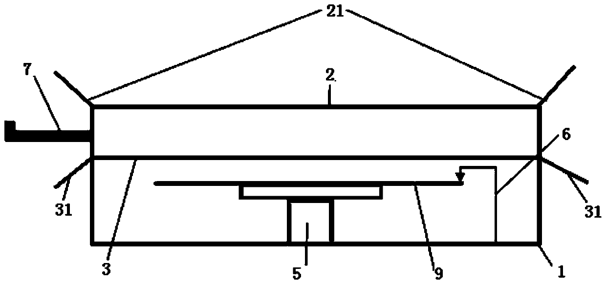
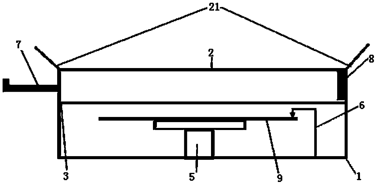
[0084] Such as figure 1 As shown, the wafer surface charge elimination device includes a shell 1, a separator 3 and an upper plate 2;
[0085] The shell 1 forms a closed cavity;
[0086] The partition 3 is fixed in the middle of the shell 1, and when it shrinks, the airtight cavity formed by the shell 1 is connected as a whole, and when it is expanded, the airtight cavity formed by the shell 1 is isolated into a closed upper chamber and a closed lower chamber;
[0087] A closed lower chamber is formed between the partition plate 3 and the side wall and the bottom plate of the shell 1, and a closed upper chamber is formed between the partition plate 3 and the side wall and the top plate of the shell 1;
[0088] The side wall of the housing 1 at the lower chamber is provided with a wafer placement door that can be opened and closed;
[0089] The upper plate 2 is arranged in the upper chamber and parallel to the separator 3;
[0090] The shell 1 is made of insulating material...
Embodiment 2
[0098] Based on the wafer surface charge elimination device of Embodiment 1, the worktable 5 is connected with a moving cylinder, and can be driven up, down and rotated by the moving cylinder.
[0099] Preferably, the wafer surface charge elimination device also includes an air pressure gauge and an air filling and pumping device 7;
[0100] The air pressure gauge is used to detect the air pressure in the upper chamber;
[0101] The air charging and pumping device 7 is used to pump and inflate the upper chamber through the ventilation interface.
[0102] Preferably, the charge measurement device 6 is installed next to the workbench 5 for detecting the charge polarity and power distribution on the surface of the wafer carried by the workbench 5 .
[0103] Preferably, the wafer surface charge elimination device also includes a controller;
[0104] The controller calculates the amount of charge that needs to be neutralized according to the charge polarity and electric charge di...
Embodiment 3
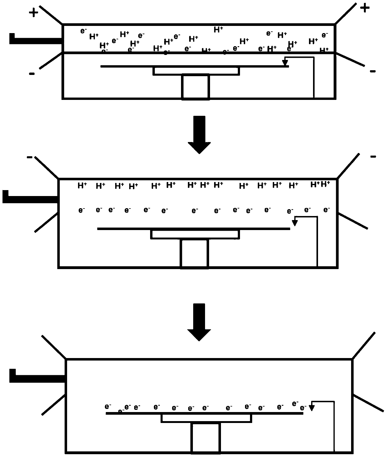
[0106] The wafer surface charge elimination method based on the wafer surface charge elimination device of embodiment two, such as figure 2 shown, including the following steps:
[0107] 1. Open the wafer placement door, place the wafer 9 to be processed on the workbench 5 by an external manipulator, and then close the wafer placement door;
[0108] 2. Expand the partition 3 to form a completely isolated upper chamber and a lower chamber;
[0109] 3. The charge measuring device 6 measures the surface charge of the wafer 9 to be processed. If the surface charge of the wafer 9 to be processed is within the set range (the set range is determined according to the acceptable range of the subsequent process), proceed to step 9, otherwise proceed to step 4 ;
[0110] 4. The controller calculates the amount of charge to be neutralized according to the charge polarity and electric charge distribution on the surface of the wafer 9 to be processed, and the corresponding pre-stored waf...
PUM
 Abstract
Description
Claims
Application Information
 - R&D
- Intellectual Property
- Life Sciences
- Materials
- Tech Scout
- Unparalleled Data Quality
- Higher Quality Content
- 60% Fewer Hallucinations
Browse by: Latest US Patents, China's latest patents, Technical Efficacy Thesaurus, Application Domain, Technology Topic, Popular Technical Reports.
© 2025 PatSnap. All rights reserved.Legal|Privacy policy|Modern Slavery Act Transparency Statement|Sitemap|About US| Contact US: help@patsnap.com