Room temperature sintering method of nano copper conductive ink
A technology of conductive ink and sintering method, which is applied in the direction of conductive pattern formation, ink, electrical components, etc., can solve the problems of not getting conductivity, etc., and achieve the effect of simple process
- Summary
- Abstract
- Description
- Claims
- Application Information
AI Technical Summary
Problems solved by technology
Method used
Image

Examples
Embodiment 1
[0027] (1) Disperse copper nanoparticles with a diameter of 11nm (prepared according to the method of I&ECR, 2018, 57) in n-octane, prepare an ink with a solid content of 30w%, put it in an ultrasonic cleaner for 2 hours, and obtain a deep red ink.
[0028] (2) Take an appropriate amount of ink on the polyethylene terephthalate (PET) film, and use the preparer to coat the film.
[0029] (3) soak the film prepared in step (2) in 10v% formic acid ethanol solution for 20s, and use formic acid to fully remove oleylamine on the surface of the particles, so that the surface of the film changes from hydrophobicity to hydrophilicity. Then wash with ethanol 3 times and blow dry.
[0030] (4) Repeat steps (2) and (3) for 3 coatings;
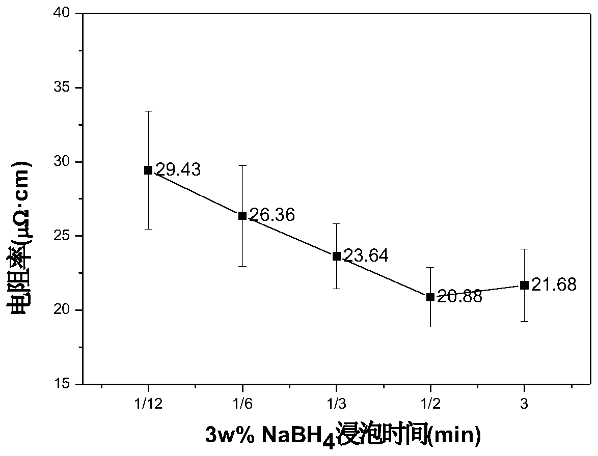
[0031] (5) soak the film of step (4) in 3w%NaBH 4 In the aqueous solution for 0.08-3min, then washed with water for 3 times, and dried.
[0032] The sheet resistance of the film was measured by a four-probe tester, the film thickness was measured by SEM...
Embodiment 2
[0034] (1) Disperse copper nanoparticles with a diameter of 11nm (prepared according to the method of I&ECR, 2018, 57) in n-octane, prepare an ink with a solid content of 30w%, put it in an ultrasonic cleaner for 2 hours, and obtain a deep red ink.
[0035] (2) Take an appropriate amount of ink on the polyethylene terephthalate (PET) film, and use the preparer to coat the film.
[0036] (3) Soak the film prepared in step (2) in a methanol solution of 10v% formic acid for 20s, and use formic acid to fully remove oleylamine on the surface of the particles, so that the surface of the film changes from hydrophobicity to hydrophilicity. Then wash with methanol 3 times and blow dry.
[0037] (4) Repeat steps (2) and (3) for 3 coatings;
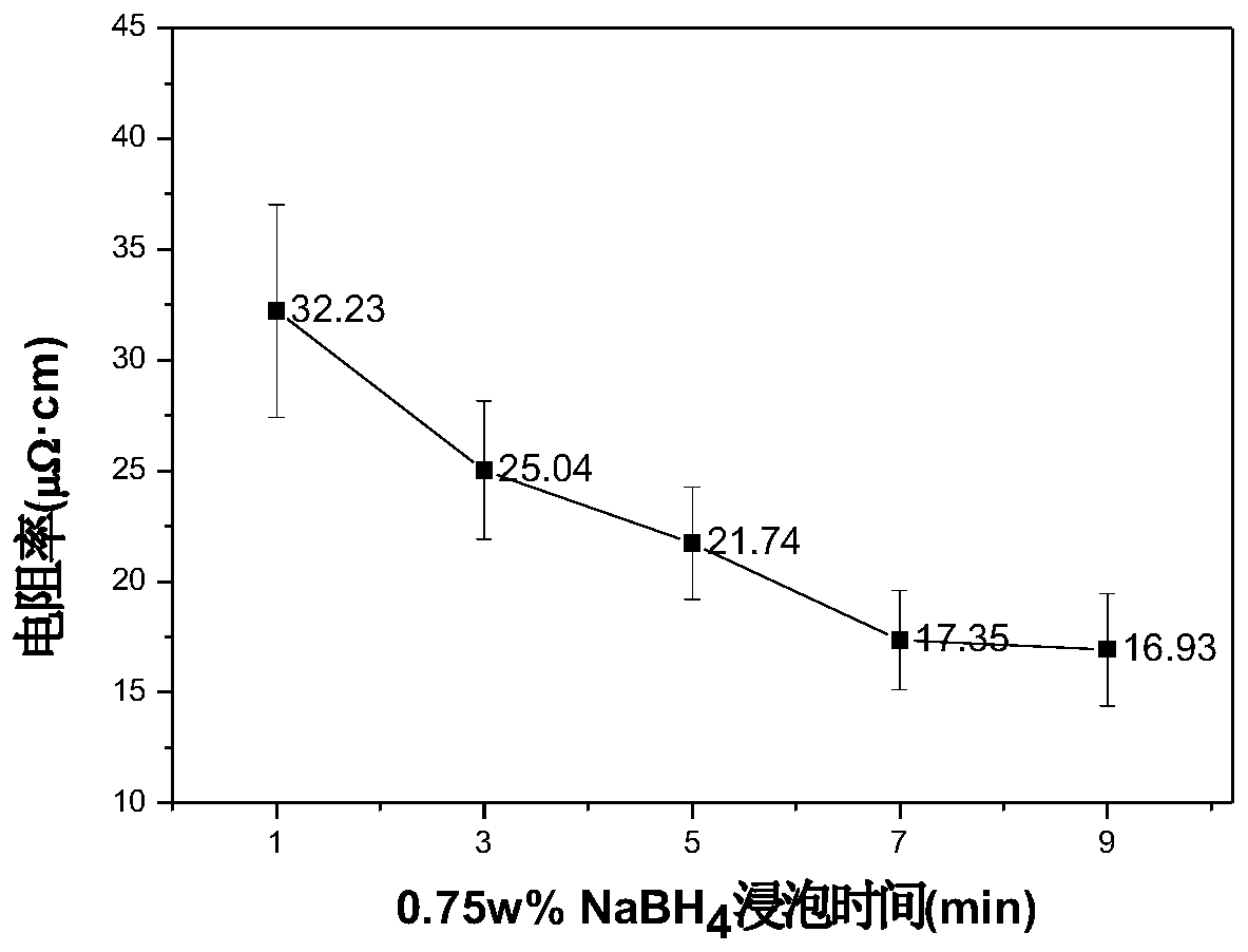
[0038] (5) soak the film of step (4) in 0.75w% NaBH 4 In the solution for 1-9min, wash with water 3 times, and dry.
[0039] The sheet resistance of the film was measured by a four-probe tester, the film thickness was measured by SEM, and the res...
Embodiment 3
[0041] 1) Disperse copper nanoparticles with a diameter of 11nm (prepared according to the method of I&ECR, 2018, 57) in n-octane, prepare an ink with a solid content of 30w%, put it in an ultrasonic cleaner for 2 hours, and obtain a deep red ink.
[0042] 2) Take an appropriate amount of ink on the polyethylene terephthalate (PET) film, and use the preparer to coat the film.
[0043] 3) Soak the membrane prepared in step 2) in a methanol solution of 10v% acetic acid for 20s, and use formic acid to fully remove oleylamine on the surface of the particles, so that the surface of the membrane changes from hydrophobic to hydrophilic. Then wash with methanol 3 times and blow dry.
[0044] 4) Repeat steps 2) and 3) to coat the film 3 times;
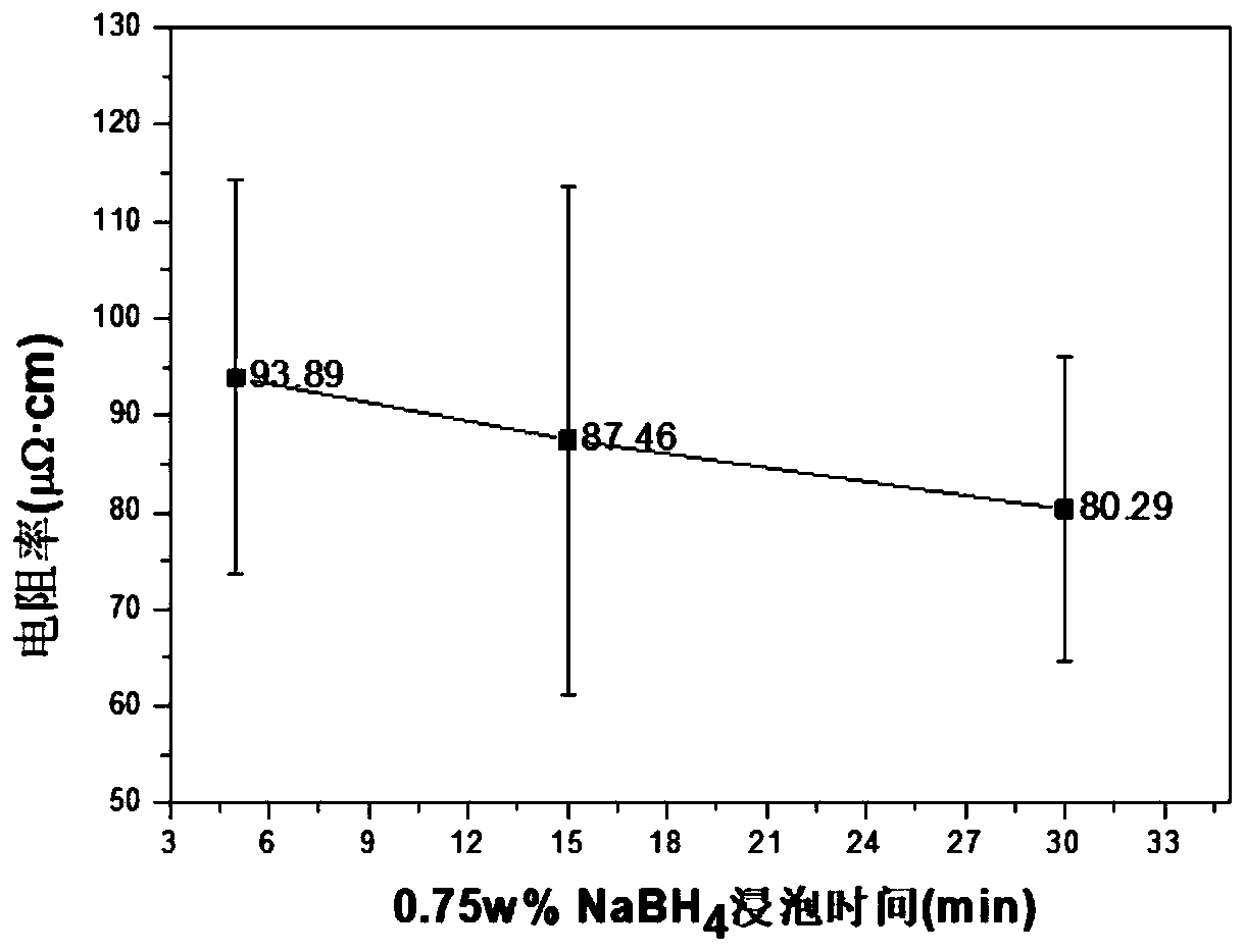
[0045] 5) Soak the film of step 4) in 0.75w% NaBH 4 In the solution for 4-30min, then wash with water 3 times, and dry.
[0046] The sheet resistance of the film was measured by a four-probe tester, the film thickness was measured by SEM, an...
PUM
 Abstract
Description
Claims
Application Information
 - R&D
- Intellectual Property
- Life Sciences
- Materials
- Tech Scout
- Unparalleled Data Quality
- Higher Quality Content
- 60% Fewer Hallucinations
Browse by: Latest US Patents, China's latest patents, Technical Efficacy Thesaurus, Application Domain, Technology Topic, Popular Technical Reports.
© 2025 PatSnap. All rights reserved.Legal|Privacy policy|Modern Slavery Act Transparency Statement|Sitemap|About US| Contact US: help@patsnap.com