
Adjustment of clamping and feeding mechanism of semiconductor silicon rod based on the principle of veneer transposition

A clamping mechanism and semiconductor technology, used in grinding racks, fine working devices, manufacturing tools, etc., can solve problems such as lack of surface contact, and achieve the effect of eliminating friction, realizing driving force and good fixation.

Active Publication Date: 2020-12-08
江苏泓顺硅基半导体科技有限公司
View PDF9 Cites 0 Cited by
  • Summary
  • Abstract
  • Description
  • Claims
  • Application Information

AI Technical Summary

Problems solved by technology

[0004] In view of the deficiencies in the prior art, the purpose of the present invention is to provide a clamping and feeding mechanism for adjusting semiconductor silicon rods based on the principle of veneer transposition, so as to solve the problem that the clamping mechanism in the prior art can only ensure that the center of the silicon rod at both ends is centered. , but it cannot guarantee that other parts of the surface are in the center of the circle during grinding, resulting in the situation that some areas of the cutting mechanism cannot be touched during the grinding and cutting process. Therefore, it is urgent to invent a clamp that can quickly adjust the grinding azimuth feed institutional issues

Method used


Image

  • Adjustment of clamping and feeding mechanism of semiconductor silicon rod based on the principle of veneer transposition
  • Adjustment of clamping and feeding mechanism of semiconductor silicon rod based on the principle of veneer transposition
  • Adjustment of clamping and feeding mechanism of semiconductor silicon rod based on the principle of veneer transposition

Examples


Embodiment

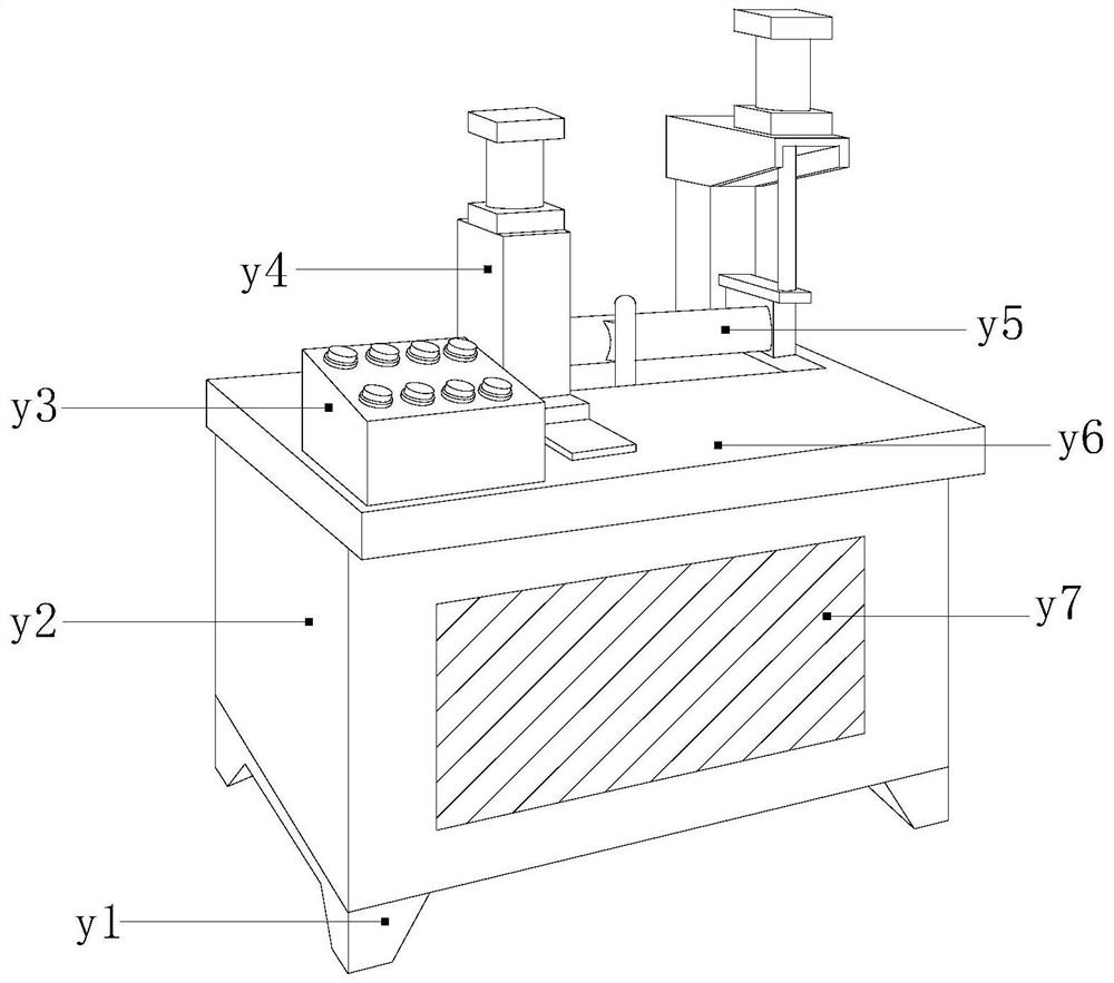
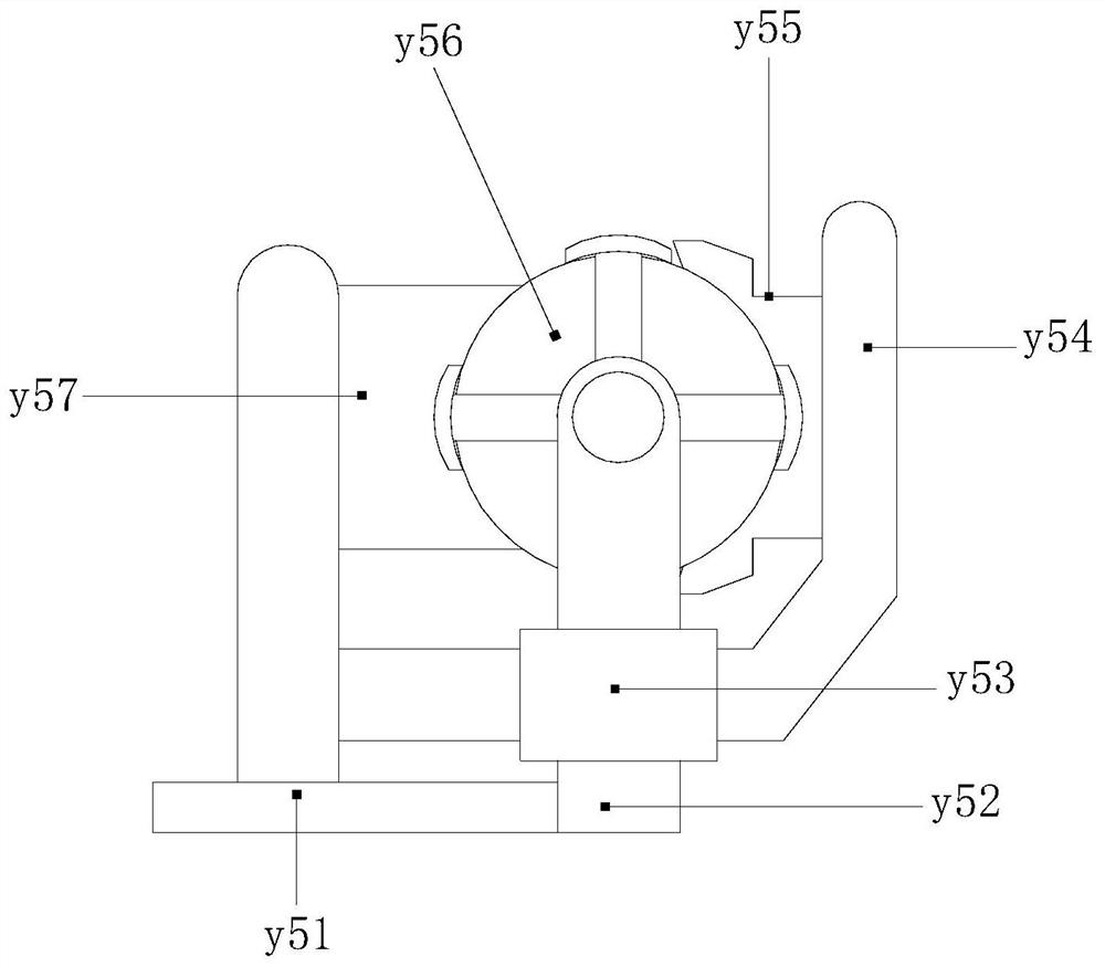
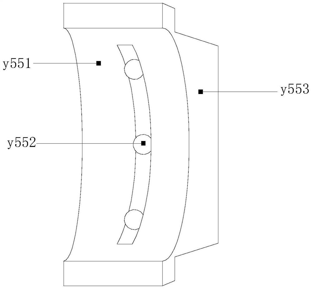
[0029] see Figure 1-Figure 6 , the present invention provides a clamping and feeding mechanism for adjusting semiconductor silicon rods based on the principle of veneer transposition. Groove y7, the heat dissipation groove y7 has a rectangular structure, and is installed on the front end of the host y2 by embedding, the bottom four corners of the host y2 are provided with fixed feet y1, and the bottom of the controller y3 is installed on the surface of the processing platform y6 by embedding At the left end, the right end of the surface of the processing platform y6 is provided with two vertical arms y4, and a clamping mechanism y5 is provided between the two vertical arms y4, and they are connected by buckling. The processing platform y6 has a rectangular structure, And it is installed on the top of the main machine y2 by means of fitting, and the main machine y2 is started by the controller y3, and the silicon rod main body y56 is placed on the clamping mechanism y5 for gri...


PUM


Abstract

The invention discloses a clamping feeding mechanism, based on the principle of veneer transposition, of adjusting semiconductor silicon rod. The clamping feeding mechanism comprises a fixing foot, ahost, a controller, a vertical arm, a clamping mechanism, a machining platform and a heat sink. The clamping mechanism fixes the main body of the silicon bar through a clamping column, and then a parallel guide sleeve positions a synchronous pull rod, so that a covering mechanism fits the right side of the main body of the silicon bar, the flatness of the main body of the silicon bar can be judgedby the covering mechanism, and finally the vertical cutting mechanism can move synchronously. The clamping feeding mechanism ensures that the real-time adjustment can be made according to the flatness in the machining process, so that timely feeding compensation is achieved, the phenomenon that some areas cannot be contacted during the grinding and cutting process is effectively avoided, the accuracy of machining is improved, and the roundness after the subsequent silicon wafer cutting is ensured.

Description

technical field [0001] The invention relates to the field of semiconductors, in particular to a clamping and feeding mechanism for adjusting semiconductor silicon rods based on the principle of veneer transposition. Background technique [0002] When making semiconductor silicon wafers, the material used is a silicon material whose quality meets the requirements of semiconductor devices, also known as silicon rods. The silicon rods are polished, sliced, and polished by equipment to make silicon wafers. The silicon rods are polished. In the process, due to various factors of poor incoming materials, the surface flatness of the silicon rods is quite different. It is necessary to divide and fix the first and last ends of the silicon rods through the clamping device, and then be driven by the equipment to rotate, and finally cooperate with the cutting mechanism. Cut into slices. There are such problems in the use of existing technologies on the market: [0003] The clamping me...

Claims


Application Information

Patent Timeline
Patent Type & Authority Patents(China)
IPC IPC(8): B24B41/02B24B41/06B24B55/06B24B55/12B28D5/00B28D5/02
CPCB24B41/02B24B41/06B24B55/06B24B55/12B28D5/0076B28D5/0082B28D5/022
Inventor 刘良国
Owner 江苏泓顺硅基半导体科技有限公司
Learn More