Ultraviolet LED epitaxial wafer and preparation method thereof

A kind of LED epitaxial wafer and ultraviolet technology, applied in the direction of electrical components, circuits, semiconductor devices, etc., can solve the problems of crystal dislocation, limit the large-scale application of glass materials, lattice mismatch, etc., achieve good conductivity and realize large-scale Production application, the effect of low production cost

Inactive Publication Date: 2019-11-08
SOUTH CHINA NORMAL UNIVERSITY +1
View PDF7 Cites 1 Cited by
  • Summary
  • Abstract
  • Description
  • Claims
  • Application Information

AI Technical Summary

Problems solved by technology

At present, the growth of GaN on ordinary glass substrates and the preparation of LEDs are both feasible. However, due to the characteristics of glass materials, it is still necessary to overcome the lattice mismatch, Major defects such as thermal mismatch, crystal dislocation, and stacking fault severely limit the large-scale application of glass materials in LED commercial production

Method used


Image

  • Ultraviolet LED epitaxial wafer and preparation method thereof
  • Ultraviolet LED epitaxial wafer and preparation method thereof

Examples


Embodiment 1

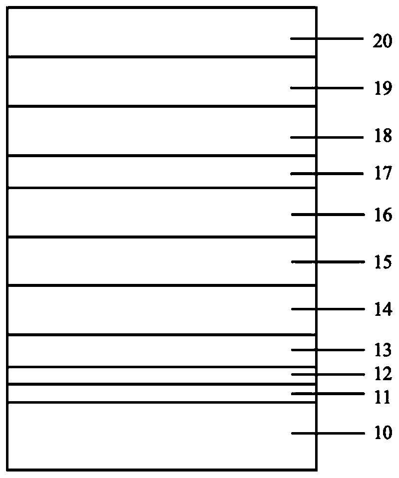
[0048] Such as figure 1 As shown, the present embodiment provides a structure of an ultraviolet LED epitaxial wafer, including:

[0049] glass substrate 10;

[0050] A copper metal layer 11 grown on the glass substrate 10, the thickness of the copper metal layer 11 is 150-300 μm;

[0051] A silver metal layer 12 grown on the copper metal layer 11, the thickness of the silver metal layer 12 is 100-300nm;

[0052] A polycrystalline AlN layer 13 grown on the silver metal layer 12, the thickness of the polycrystalline AlN layer 13 is 30-100 nm;

[0053] A single crystal AlN layer 14 grown on the polycrystalline AlN layer 13, the thickness of the single crystal AlN layer 14 is 50-200 nm;

[0054] A non-doped AlGaN layer 15 grown on the single crystal AlN layer 14, the thickness of the non-doped AlGaN layer 14 is 500-1000 nm;

[0055] An n-type doped AlGaN layer 16 grown on the non-doped AlGaN layer 15, the thickness of the n-type doped AlGaN layer 15 is 3000-5000 nm;

[0056] ...

Embodiment 2

[0061] The preparation method of the ultraviolet LED epitaxial wafer of the present embodiment comprises:

[0062] (1) Selection of substrate and its crystal orientation: use ordinary glass substrate;

[0063] (2) Substrate surface polishing and cleaning treatment;

[0064] The surface of the substrate is polished and cleaned, specifically:

[0065] Put the glass substrate into deionized water and ultrasonically clean it at room temperature for 3 minutes to remove the dirt particles on the surface of the glass substrate, then wash it with acetone and ethanol in order to remove the surface organic matter, and dry it with high-purity dry nitrogen;

[0066] (3) Growth of the copper metal layer: Firstly, the glass substrate was treated with plasma for 3 minutes under the condition of oxygen atmosphere, and then the glass substrate was placed in the electroplating solution, and a copper layer with a thickness of 150 μm was prepared at room temperature. metal layer;

[0067] (4) ...


PUM

PropertyMeasurementUnit
Thicknessaaaaaaaaaa
Thicknessaaaaaaaaaa
Thicknessaaaaaaaaaa

Abstract

The invention discloses an ultraviolet LED epitaxial wafer, which comprises a glass substrate, and a metal layer, a polycrystalline AlN layer, a single crystal AlN layer, an undoped AlGaN layer, an n-type doped AlGaN layer, a multi-quantum well layer, an AlGaN electron blocking layer, a p-type doped AlGaN layer, and a p-type doped GaN layer sequentially growing on the glass substrate. The invention also discloses an ultraviolet LED epitaxial wafer preparation method. Based on the characteristics of each layer, an electroplating method, a magnetron sputtering method, a physical vapor depositionmethod and a molecular beam epitaxial growth technology are combined. The GaN material with less defects and high quality can grow, the substrate is easy to remove, heat conduction and electrical conductivity are good, and the light emitting performance is high. The production process is simple, the cost is low, the reproducibility is achieved, and large-scale production application can be realized.

Description

technical field [0001] The invention relates to an LED epitaxial wafer and a preparation method thereof, in particular to an ultraviolet LED epitaxial wafer grown on a glass substrate and a preparation method thereof. Background technique [0002] GaN-based ultraviolet LED epitaxial materials and devices, as the key to the third-generation semiconductor materials and devices, can be applied to sterilization, medical equipment and other fields, and have developed extremely rapidly in recent years. [0003] At present, high-quality GaN materials are generally produced by heteroepitaxial methods. Since different substrates will directly affect the lattice quality of the grown epitaxial layer, the choice of substrate is very important. Generally, the selection of substrates needs to follow the following principles, such as lattice constant matching, thermal expansion coefficient matching, reasonable price, etc. In addition, the selection of different substrates will cause differ...

Claims


Application Information

Patent Timeline
IPC IPC(8): H01L33/12H01L33/06H01L33/32H01L33/46H01L33/00
CPCH01L33/007H01L33/06H01L33/12H01L33/32H01L33/46H01L33/0093
Inventor 高芳亮李述体李晓航罗幸君张柏林刘青
Owner SOUTH CHINA NORMAL UNIVERSITY
Why Eureka
Try Eureka