Joining molded article and method for manufacturing same
A molding and precursor technology, applied in manufacturing tools, printed circuit manufacturing, welding equipment, etc., can solve the problem of difficult high-strength semiconductor chip components being bonded to the substrate, and achieve the effect of high thermal conductivity
- Summary
- Abstract
- Description
- Claims
- Application Information
AI Technical Summary
Problems solved by technology
Method used
Image

Examples
no. 1 Embodiment approach >
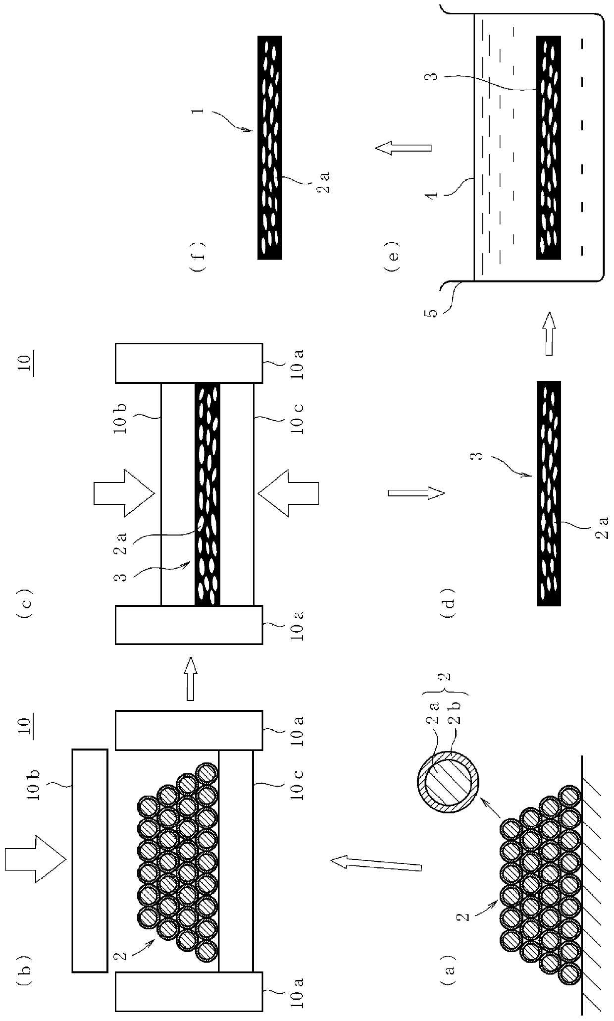
[0015] Such as figure 1 As shown, regarding the molded body 1 for joining according to the first embodiment of the present invention, the Cu core Sn shell powder 2 is press-molded to produce a granular or flake shape with a thickness of 20 to 400 μm.
[0016] 〔Cu core Sn shell powder〕
[0017] Such as figure 1 As shown in the enlarged view of (a), the Cu core Sn shell powder 2 as the raw material of the molded body for joining is composed of a core 2a and a shell 2b, wherein the core 2a is made of Cu, and the shell 2b covers the core 2a and Composed of Sn. The average particle size of the Cu core Sn shell powder 2 is 0.5 to 50 μm, preferably 1.0 to 20 μm. It is known that when the average particle size is less than 0.5 μm as the lower limit, it is not only difficult to produce a molded body precursor with a uniform density when performing press forming or roll forming described later, but also in normal operations such as 25° C. At the temperature of the material, Cu diffu...
no. 2 Embodiment approach >
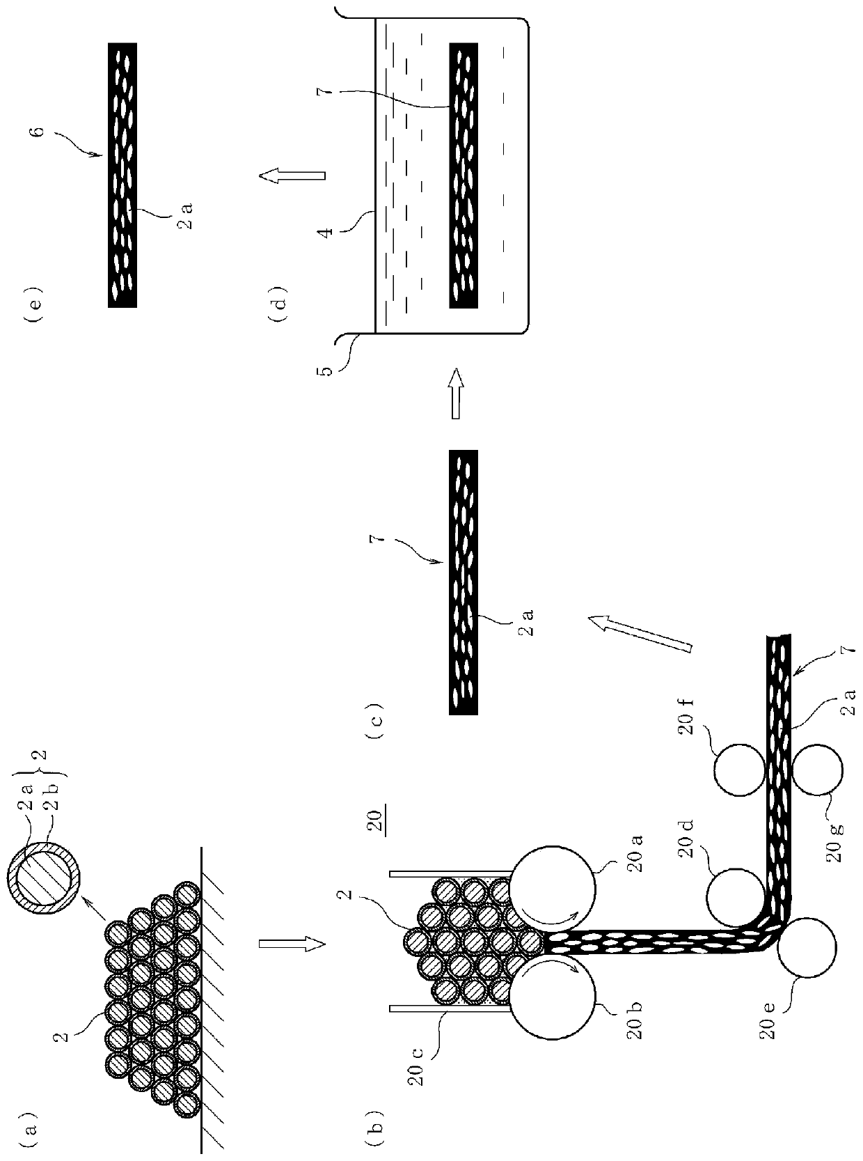
[0030] Such as figure 2 As shown, the molded body 6 for joining according to the second embodiment of the present invention uses the same Cu core Sn shell powder 2 as that of the first embodiment ( figure 2 (a)) is roll-formed to produce flakes or pellets with a thickness of 20 to 400 μm.
[0031] 〔Manufacture of molded body precursor〕
[0032] Such as figure 2 As shown in (b), in an inert gas atmosphere such as nitrogen or argon, Cu core Sn shell powder 2 is subjected to powder roll molding with a powder rolling machine 20 to produce a molded body precursor 7 . The powder rolling machine 20 has a pair of cylindrical rolls 20a, 20b and a hopper 20c connected to the upper surfaces of these rolls. The roller 20a and the roller 20b rotate in opposite directions to each other, and at figure 2 In the process, the Cu core Sn shell powder 2 thrown into the hopper 20c is rolled downward, and the rolling body is comprised so that it may be guided in the horizontal direction by ...
Embodiment 1
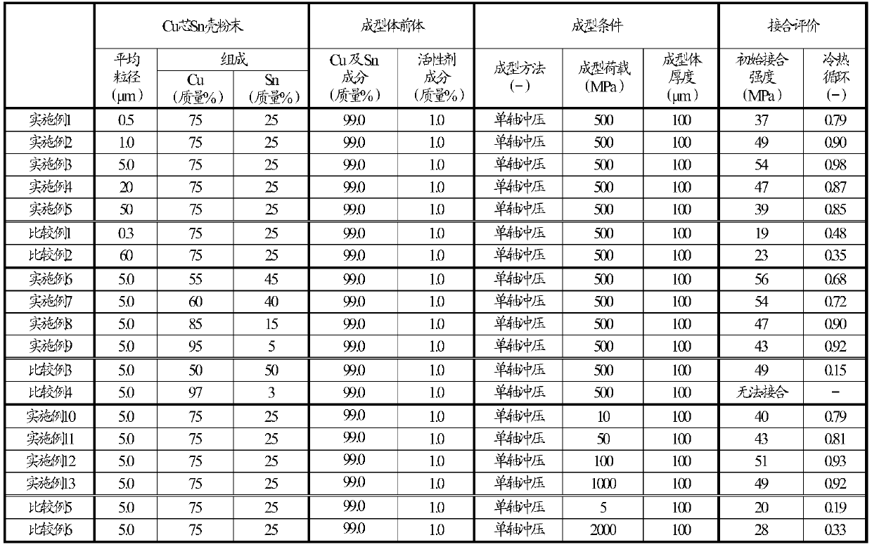
[0042] A Cu core Sn shell powder having an average particle diameter of 0.5 μm, a Cu ratio of 75% by mass, and a Sn ratio of 25% by mass was prepared. Here, the compositional ratio of Cu and Sn in the Cu core Sn shell powder was measured by ICP emission spectroscopy (manufactured by Thermo Fisher Scientific, iCAP-6500Duo). In addition, the crystal structure of the core-shell structure is mainly composed of Cu and Sn, and was confirmed by a powder X-ray diffraction method (manufactured by PANalytical, multi-purpose X-ray diffractometer Empyrean). The above-mentioned Cu core Sn shell powder was uniaxially pressed using a die at 500 MPa for 300 seconds to obtain a square (□) granular molded body precursor with a thickness of 100 μm and a side length of 3 mm.
[0043] On the other hand, a liquid activator-containing material in which a general-purpose flux (92MS manufactured by Arakawa Chemical Industries, Ltd.) was diluted with an organic solvent α-terpineol was obtained so that ...
PUM
| Property | Measurement | Unit |
|---|---|---|
| thickness | aaaaa | aaaaa |
| particle diameter | aaaaa | aaaaa |
| particle size | aaaaa | aaaaa |
Abstract
Description
Claims
Application Information
 - R&D
- Intellectual Property
- Life Sciences
- Materials
- Tech Scout
- Unparalleled Data Quality
- Higher Quality Content
- 60% Fewer Hallucinations
Browse by: Latest US Patents, China's latest patents, Technical Efficacy Thesaurus, Application Domain, Technology Topic, Popular Technical Reports.
© 2025 PatSnap. All rights reserved.Legal|Privacy policy|Modern Slavery Act Transparency Statement|Sitemap|About US| Contact US: help@patsnap.com