Metalized film and production method therefor
A technology of metallized film and manufacturing method, applied in the direction of chemical instruments and methods, metal pattern materials, metal layered products, etc., can solve the problems of poor productivity and achieve the effect of smooth conduction loss and stable passability
- Summary
- Abstract
- Description
- Claims
- Application Information
AI Technical Summary
Problems solved by technology
Method used
Image


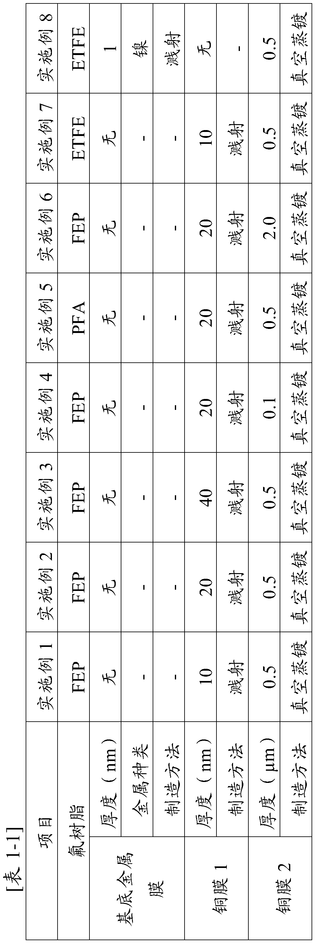
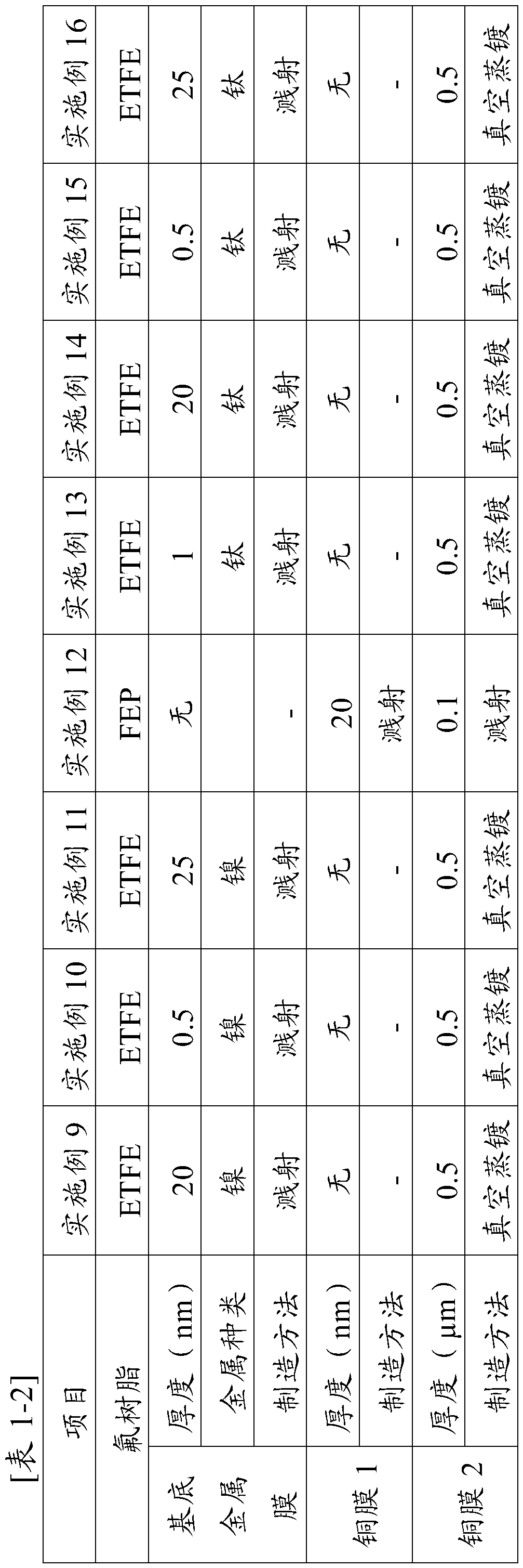
Examples
Embodiment
[0046] Hereinafter, although this invention is demonstrated concretely based on an Example, this invention is not limited to these Examples.
Embodiment approach 1
[0048] A plating resist is formed on the copper film 2 of the metallized film of the present invention. As a plating resist, "PMER P-LA900PM" of Tokyo Ohka Co., Ltd. was used, and a plating resist having a wiring pattern of L / S=10 / 10 μm was formed with a resist thickness of 20 μm. The electrolytic Cu plating solution was set to copper sulfate pentahydrate 50g / L, sulfuric acid 200g / L, chlorine 50ppm, additives of Meltex Co., Ltd. "Copper Gleam" ST-901A 2ml / L, "Copper Gleam" ST-901B 20ml / L liquid. In terms of electroplating conditions, by jet flow, 1.0A / dm 2 The current density is such that the thickness of the copper film 3 is 10 µm thick. After electrolytic plating, the plating resist is removed with an alkaline stripper, and then the copper film 1 and copper film 2 for power supply between the wirings are removed using a hydrogen peroxide-sulfuric acid-based etching solution to form wirings.
[0049] It should be noted that, in the case of using a metallized film formed w...
Embodiment approach 2
[0052] Using the same electrolytic plating solution as in Embodiment 1 for wiring formation, the plating conditions were jet flow, 1.0A / dm 2 A current density of 15 μm thick copper film 3 was formed on the entire surface of the copper film 2 of the metallized film of the fluororesin film.
[0053] Next, an etching resist is formed on the above-mentioned copper film 3 . As a plating resist, Tokyo Ohka Co., Ltd. "PMER P-LA900PM" was used, and the etching resist which formed the wiring pattern of L / S=50 / 50 micrometer with a resist thickness of 20 micrometers was used. After the plating resist was formed, the copper film 1, the copper film 2, and the copper film 3 were etched by a shower method using a ferric chloride-based etching solution. After etching, the etching resist is removed with an alkaline stripper to form wiring.
[0054] (Measurement of Surface Roughness)
[0055] The surface roughness Ra is the arithmetic mean roughness defined in JIS B 0601-1994, which is the f...
PUM
| Property | Measurement | Unit |
|---|---|---|
| surface roughness | aaaaa | aaaaa |
| thickness | aaaaa | aaaaa |
| thickness | aaaaa | aaaaa |
Abstract
Description
Claims
Application Information
 - R&D
- Intellectual Property
- Life Sciences
- Materials
- Tech Scout
- Unparalleled Data Quality
- Higher Quality Content
- 60% Fewer Hallucinations
Browse by: Latest US Patents, China's latest patents, Technical Efficacy Thesaurus, Application Domain, Technology Topic, Popular Technical Reports.
© 2025 PatSnap. All rights reserved.Legal|Privacy policy|Modern Slavery Act Transparency Statement|Sitemap|About US| Contact US: help@patsnap.com