MOSFET device with silicon carbide inverted T-shaped masking layer structure and preparation method thereof

A masking layer, silicon carbide technology, applied in the field of microelectronics, can solve the problems affecting the forward blocking characteristics of the device, and achieve the effects of reducing the JFET effect, reducing the electric field concentration, and improving the breakdown voltage

Pending Publication Date: 2019-09-24
陕西半导体先导技术中心有限公司
View PDF0 Cites 3 Cited by
  • Summary
  • Abstract
  • Description
  • Claims
  • Application Information

AI Technical Summary

Problems solved by technology

[0003] In the traditional groove gate structure MOSFET, the electric field concentration at the corner of the gate dielectric layer leads to the breakdown of the gate dielectric layer, causing the device to break down below the rated breakdown voltage, which seriously affects the forward blocking characteristics of the device

Method used


Image

  • MOSFET device with silicon carbide inverted T-shaped masking layer structure and preparation method thereof
  • MOSFET device with silicon carbide inverted T-shaped masking layer structure and preparation method thereof
  • MOSFET device with silicon carbide inverted T-shaped masking layer structure and preparation method thereof

Examples


Embodiment 1

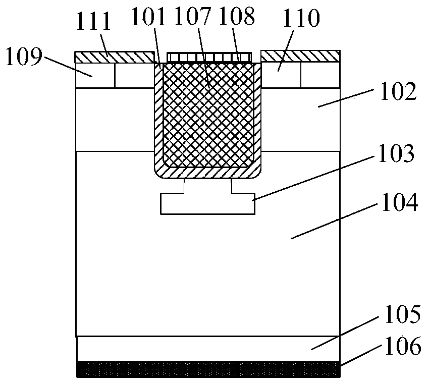
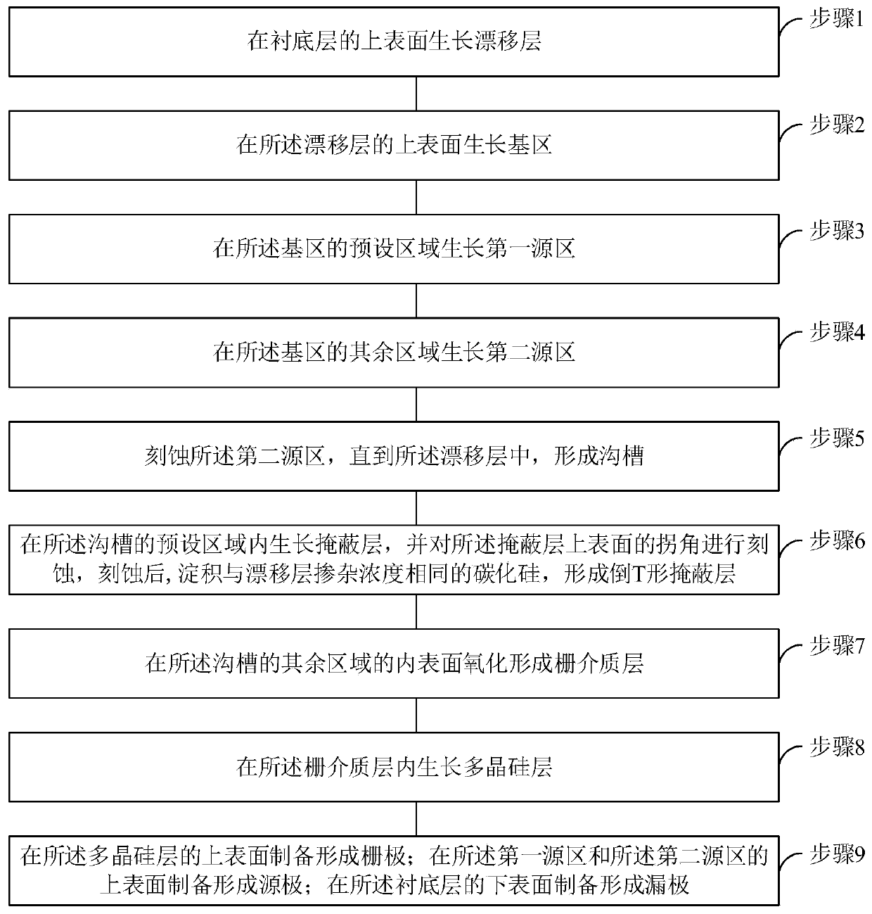
[0049] See figure 1 , figure 1 A schematic cross-sectional structure diagram of a MOSFET device with a silicon carbide inverted T-shaped mask layer structure provided by an embodiment of the present invention.

[0050] A MOSFET device with a silicon carbide inverted T-shaped masking layer 103 structure, comprising:

[0051] gate dielectric layer 101;

[0052] a base region 102 located on both sides of the gate dielectric layer 101;

[0053] a masking layer 103 located on the lower surface of the gate dielectric layer 101;

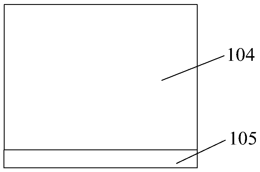
[0054] a drift layer 104 located on the lower surface of the base region 102 and the masking layer 103;

[0055] a substrate layer 105 located on the lower surface of the drift layer 104;

[0056] The drain 106 is located on the surface of the substrate layer 105;

[0057] a polysilicon layer 107 located on the inner surface of the gate dielectric layer 101;

[0058] The gate 108 is located on the upper surface of the polysilicon layer 107 .

[0059...


PUM


Abstract

The invention relates to an MOSFET device with a silicon carbide inverted T-shaped marking layer structure and a preparation method thereof. The MOSFET device comprises a gate dielectric layer, a base region, a masking layer, a drift layer, a substrate layer, a drain electrode, a polycrystalline silicon layer, a grid electrode, a first source region, a second source region and a source electrode, wherein the base region is located at two sides of the gate dielectric layer; the masking layer is located on the lower surface of the gate dielectric layer; the drift layer is located on the lower surfaces of the base region and the masking layer; the substrate layer is located on the lower surface of the drift layer; the drain electrode is located on the surface of the substrate layer; the polycrystalline silicon layer is located on the inner surface of the gate dielectric layer; the grid electrode is located on the upper surface of the polycrystalline silicon layer; the first source region is located on the upper surface of a part of the base region; the second source region is located on the upper surface of the rest of the base region; and the source electrode is located on the upper surfaces of the first source region and the second source region. According to the MOSFET device, the electric field distribution at the corner of the gate dielectric layer is changed through the P+ type masking layer at the bottom of the trench gate, the electric field concentration at the corner of the device is reduced, the breakdown voltage of the device is improved, and the reliability of the device is improved.

Description

technical field [0001] The invention belongs to the technical field of microelectronics, and in particular relates to a MOSFET device with a silicon carbide inverted T-shaped masking layer structure and a preparation method thereof. Background technique [0002] Silicon carbide, a wide bandgap semiconductor material, has excellent physical and chemical properties such as large bandgap width, high critical breakdown electric field, high thermal conductivity and high electron saturation drift velocity, and is suitable for high temperature, high pressure, high power, and radiation resistance semiconductor devices. In the field of power electronics, power MOSFET devices have been widely used. It has the characteristics of simple gate drive and short switching time. [0003] In the traditional groove gate structure MOSFET, the electric field concentration at the corner of the gate dielectric layer leads to the breakdown of the gate dielectric layer, causing the breakdown of the ...

Claims


Application Information

Patent Timeline
Patent Type & Authority Applications(China)
IPC IPC(8): H01L29/06H01L21/336H01L29/78
CPCH01L29/0623H01L29/0684H01L29/66068H01L29/7813
Inventor 宋庆文张玉明白瑞杰汤晓燕袁昊何艳静何晓宁韩超
Owner 陕西半导体先导技术中心有限公司
Why Eureka
Try Eureka