PCB mounting process
A PCB board and mounting technology, applied in the field of PCB board mounting technology, can solve the problems of poor thermal conductivity of tin, unfavorable overall heat dissipation of components, and difficulty in heat dissipation of components
- Summary
- Abstract
- Description
- Claims
- Application Information
AI Technical Summary
Problems solved by technology
Method used
Image

Examples
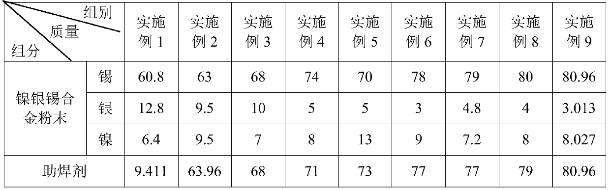
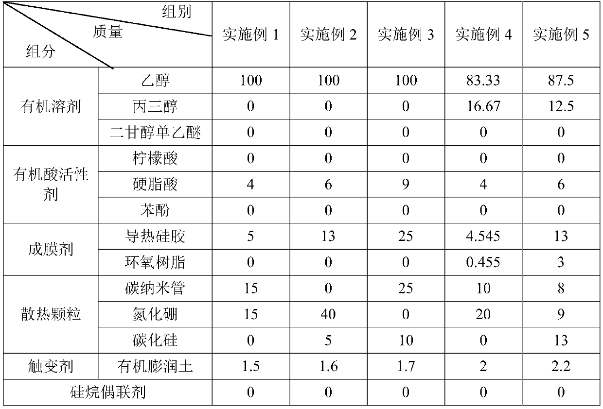
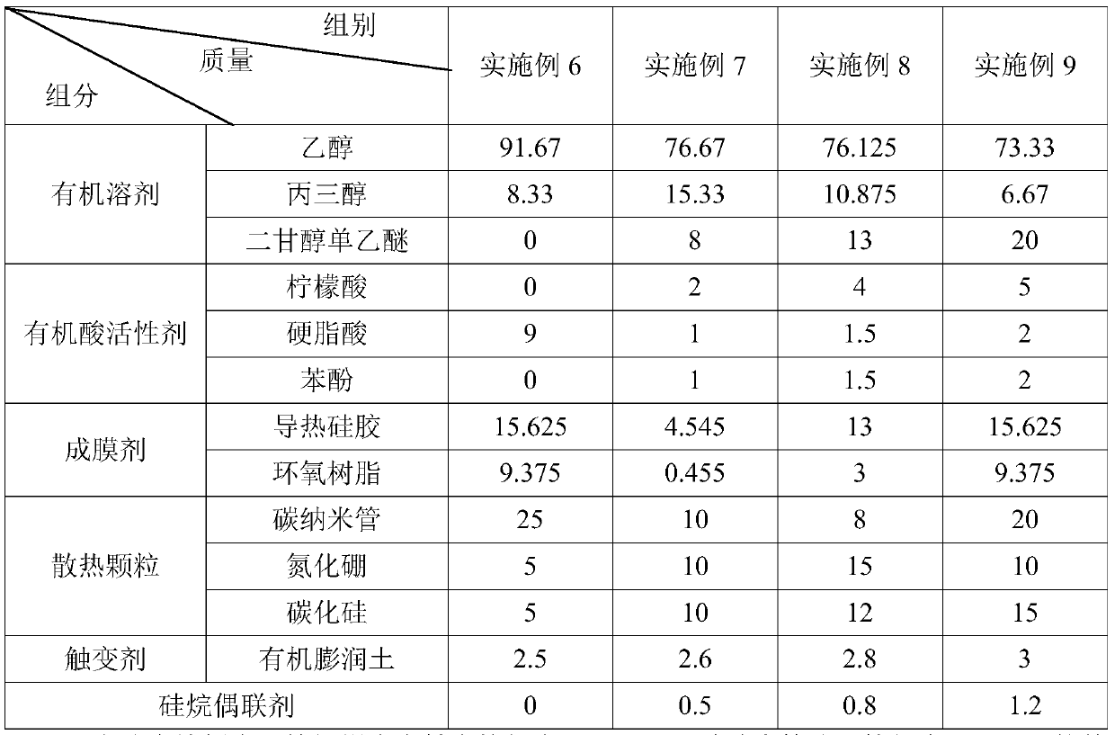
Embodiment 1-9
[0060] Embodiment 1-9: a PCB board mounting process, comprising the following steps:
[0061] Pretreatment: Spray a 75% ethanol solution on the PCB;
[0062] S1: Place a stencil on side A of the PCB, print solder paste and scrape off the solder paste on the surface of the stencil, and mount components;
[0063] S2: Pass the PCB board A side up through the reflow oven, and reflow solder the A side;
[0064] S3: Place a stencil on the B side of the PCB, print solder paste and scrape off the solder paste on the surface of the stencil, and mount the components;
[0065] S4: Pass the PCB board A side up through the reflow oven, and reflow solder the B side;
[0066] S5: After the solder paste on the A side and the B side are solidified, scrape and coat the thermal conductive silicone grease on the solder on the A side and the B side;
[0067] Among them, the reflow furnace includes a heating zone, a reflow soldering zone, and a cooling zone in sequence. The starting temperature ...
Embodiment 10
[0079] Embodiment 10: a PCB board mounting process, the difference from Embodiment 9 is that the PCB board mounting process includes the following steps:
[0080] In the pretreatment, spraying concentration is 80% ethanol aqueous solution on PCB board;
[0081] The initial temperature of the soldering zone in the reflow furnace is 180±1°C, and the PCB board stays in the soldering zone for 70s.
Embodiment 11
[0082] Embodiment 11: a PCB board mounting process, the difference from Embodiment 9 is that the PCB board mounting process includes the following steps:
[0083] In the pretreatment, spraying a concentration of 85% ethanol solution on the PCB;
[0084] The initial temperature of the soldering zone in the reflow furnace is 182±1°C, and the PCB board stays in the soldering zone for 70s.
PUM
| Property | Measurement | Unit |
|---|---|---|
| Particle size | aaaaa | aaaaa |
| Diameter | aaaaa | aaaaa |
| Particle size | aaaaa | aaaaa |
Abstract
Description
Claims
Application Information
 - Generate Ideas
- Intellectual Property
- Life Sciences
- Materials
- Tech Scout
- Unparalleled Data Quality
- Higher Quality Content
- 60% Fewer Hallucinations
Browse by: Latest US Patents, China's latest patents, Technical Efficacy Thesaurus, Application Domain, Technology Topic, Popular Technical Reports.
© 2025 PatSnap. All rights reserved.Legal|Privacy policy|Modern Slavery Act Transparency Statement|Sitemap|About US| Contact US: help@patsnap.com