A method for realizing ultra-broadband light absorption and a composite microstructure
A composite microstructure and ultra-broadband technology, applied in optics, optical components, instruments, etc., can solve the problems of limited number of microstructure resonant units and increase the difficulty of preparation, and achieve high polarization-insensitive broadband absorption performance, excellent broadband light Absorption performance, the effect of enhancing absorption efficiency
- Summary
- Abstract
- Description
- Claims
- Application Information
AI Technical Summary
Problems solved by technology
Method used
Image
Examples
Embodiment 1
[0038] Example 1: Designing an ultra-broadband wave absorber in the visible-near-infrared band using metal / dielectric composite microstructures
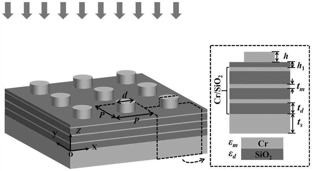
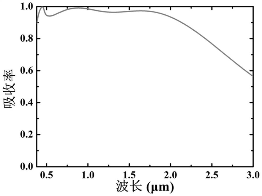
[0039] Using metal / dielectric composite microstructure to design an ultra-broadband absorber in the visible-near-infrared band, the schematic diagram is as follows figure 1 shown. figure 1 It is a schematic diagram of the metal / dielectric composite microstructure in an embodiment of the present invention. The selected metal microstructure is a nano-pillar array, and the selected metal and dielectric materials are chromium (Cr) and silicon dioxide (SiO2) respectively. 2 ). where P is the period of the nanopillar array, d is the diameter of the nanopillar, h is the height of the nanopillar, h 1 for SiO 2 The thickness of the buffer layer, a total of 3 pairs of Cr / SiO 2 Multilayer stack, t m is the thickness of the metal Cr film, t d for SiO 2 The thickness of the dielectric film layer, the substrate is a Cr film with a sufficien...
Embodiment 2
[0042] Example 2: Broadband near-field reflection and light field localization induced by metal-dielectric periodic film stacks
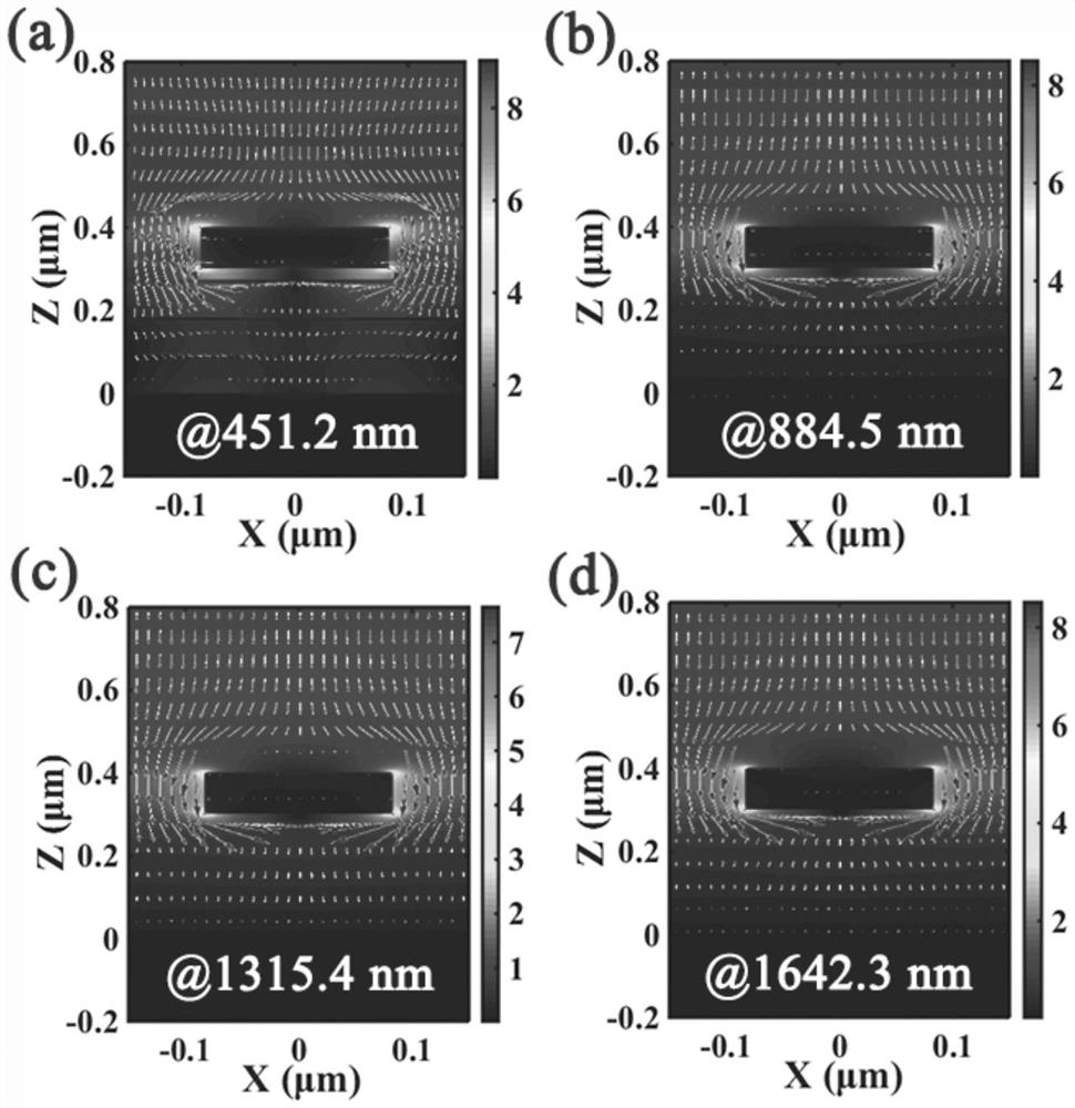
[0043] Based on the calculation results of Example 1, in order to clarify the broadband light absorption mechanism corresponding to this structure, in figure 2 Under the parameter conditions of , in the band of broadband light absorption, four light absorption wavelengths with large difference are selected in turn along the wavelength increasing direction, and the strict coupled wave method is used to calculate the normalized electric field intensity distribution and energy flow direction corresponding to the structure. distribution, get image 3 .
[0044] image 3 is the normalized electric field intensity distribution and energy flow direction distribution of different wavelengths in an embodiment of the present invention, wherein the chromaticity bar represents the amplitude of the normalized electric field intensity, the arrow indicates the ...
Embodiment 3
[0046] Example 3: Angle-insensitive absorption phenomenon of metal / dielectric composite microstructure ultra-broadband absorber
[0047] Based on the metal / dielectric composite microstructure ultra-broadband absorber in Example 1, while the structural parameters remain unchanged, the incident angle is changed. For TM polarization and TE polarization, respectively, the strict coupled wave method is used to calculate the change of the absorption spectrum with the incident angle. curve, get Figure 4 .
[0048] Figure 4 is the variation curve of the absorption spectrum with the incident angle in an embodiment of the present invention, and the structural parameters are the same as figure 2 same. (a) corresponds to TM polarization; (b) corresponds to TE polarization. from Figure 4 It can be seen that when the incident angle increases from 0° to 60°, the absorber still has a broadband light absorption effect. In particular, for the TM polarization case, when the incident an...
PUM
| Property | Measurement | Unit |
|---|---|---|
| thickness | aaaaa | aaaaa |
Abstract
Description
Claims
Application Information
 - R&D
- Intellectual Property
- Life Sciences
- Materials
- Tech Scout
- Unparalleled Data Quality
- Higher Quality Content
- 60% Fewer Hallucinations
Browse by: Latest US Patents, China's latest patents, Technical Efficacy Thesaurus, Application Domain, Technology Topic, Popular Technical Reports.
© 2025 PatSnap. All rights reserved.Legal|Privacy policy|Modern Slavery Act Transparency Statement|Sitemap|About US| Contact US: help@patsnap.com


