Red light semiconductor laser based on GexSi<1-x> variable lattice constant matrix

A lattice constant, laser technology, applied in semiconductor lasers, lasers, laser parts and other directions, can solve the problems of poor device characteristics, high light decay, complex generation and migration, etc., to achieve improved output power and photoelectric conversion efficiency, reliable Good performance and the effect of reducing tensile strain

Inactive Publication Date: 2019-08-23
XIAN UNIV OF TECH
View PDF8 Cites 1 Cited by
  • Summary
  • Abstract
  • Description
  • Claims
  • Application Information

AI Technical Summary

Problems solved by technology

However, due to the narrow conduction band offset between the tensile strain GaInP and AlGaInP heterojunctions, the electrons in the active layer overflow to the confinement layer, making it difficult to work at high power and high temperature of the laser; the tensile strain GaInP material is more durable than the compressive strain material More crystal defects make the generation and migration of internal defects more complicated; the excess heat generated by low photoelectric conversion efficiency will rapidly degrade the photoelectric characteristics of the device, making it difficult to achieve continuous high-power output at high temperatures; high photon energy makes The laser cavity surface bears a higher energy density, and the optical catastrophe damage of the cavity surface of the device is more likely to occur
Although the production of 625nm and 630nm semiconductor lasers has been realized experimentally, the device characteristics are too poor, the light attenuation is too much, and the cost performance, output power and conversion efficiency are difficult to meet the requirements of the current laser display technology and red light medical care applications for shorter wavelength red lasers. Optical Laser Requirements

Method used


Image

  • Red light semiconductor laser based on GexSi&lt;1-x&gt; variable lattice constant matrix
  • Red light semiconductor laser based on GexSi&lt;1-x&gt; variable lattice constant matrix
  • Red light semiconductor laser based on GexSi&lt;1-x&gt; variable lattice constant matrix

Examples


Embodiment 1

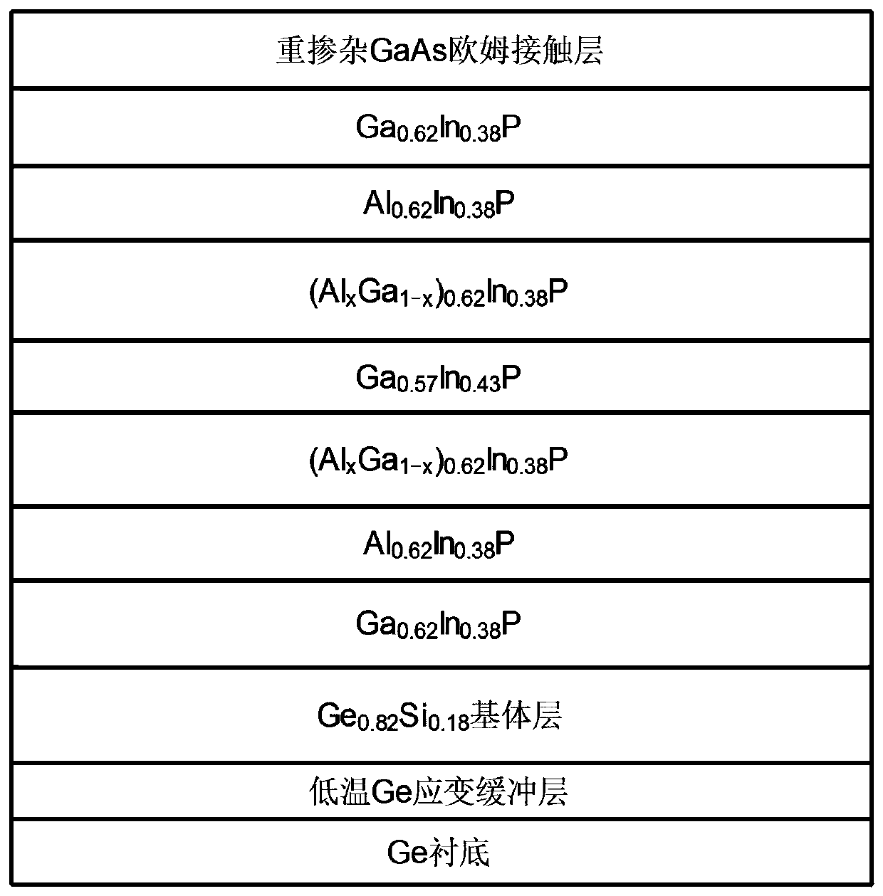
[0036] refer to figure 2 , is based on the Ge substrate Ge of the embodiment 1 of the present invention x Si 1-x Schematic diagram of the structure of the 620nm red semiconductor laser in the substrate layer. In Example 1, the cavity length of the entire semiconductor laser is 1.5 mm, the stripe width of the current injection zone is 120 μm, and the cavity surface is not coated. The device structure is a Ge substrate, a low-temperature Ge strained buffer layer, and a Ge 0.82 Si 0.18 Base layer, Ga 0.62 In 0.38 P buffer layer, Al 0.62 In 0.38 P lower confinement layer, (Al x Ga 1-x ) 0.62 In 0.38 P lower waveguide layer, (Al x Ga 1-x ) 0.62 In 0.38 P upper waveguide layer, Al 0.62 In 0.38 Confinement layer on P, Ga 0.62 In 0.38 P barrier layer, heavily doped GaAs ohmic contact layer. where the quantum well region is compared to Ge 0.82 Si 0.18 The substrate lamination strain is 0.4% Ga 0.57 In 0.43 P layer, the thickness of the well is 8nm.

[0037] ...


PUM

PropertyMeasurementUnit
Layer thicknessaaaaaaaaaa
Thicknessaaaaaaaaaa

Abstract

The invention discloses a red light semiconductor laser based on a GexSi<1-x> variable lattice constant matrix. The laser structurally comprises an N-surface electrode, a germanium substrate, a strainbuffer layer, a germanium-silicon matrix layer, a buffer layer, a lower limiting layer, a lower waveguide layer, a quantum well, a quantum barrier, an upper waveguide layer, an upper limiting layer,a barrier layer, a dielectric film, an ohmic contact layer and a P-surface electrode in sequence from bottom to top. According to the red-light semiconductor laser, the tension strain of the quantum well is reduced while the active region lasing wavelength is shortened, the problem that the active region with large tension strain has many defects in an ultra-short wavelength red-light laser can besolved, and meanwhile, the output power and the photoelectric conversion efficiency of a band laser are also improved.

Description

technical field [0001] The invention belongs to the technical field of semiconductor lasers, in particular to a Ge-based x Si 1-x Red semiconductor laser with variable lattice constant matrix. Background technique [0002] Red light semiconductor lasers are widely used in laser storage, laser display, virtual reality, laser medical beauty and other fields, but the red light lasers studied before are mainly concentrated in the 655nm-680nm band. The demand for shorter-wavelength red lasers continues to increase, and the development of 638nm-642nm short-wavelength red light, and even 620nm-635nm ultra-short-wavelength red semiconductor lasers has once again become one of the hot spots in the field of semiconductor optoelectronics. [0003] Laser display has superior picture quality and frame advantages, and also has the advantages of rich colors, high color saturation, long life, low power consumption, energy saving and environmental protection, and light weight. The advanta...

Claims


Application Information

Patent Timeline
IPC IPC(8): H01S5/343H01S5/32
CPCH01S5/3224H01S5/34326
Inventor 林涛齐玥邓泽军赵荣进马泽坤宁少欢
Owner XIAN UNIV OF TECH
Why Eureka
Try Eureka