Display device, display system and manufacturing method

A display device and display panel technology, applied in static indicators, nonlinear optics, optics, etc., can solve the problems of display device short circuit, increased coupling capacitance, circuit misconnection, etc., to reduce wiring density, reduce short circuit, To avoid the effect of increased coupling capacitance

Pending Publication Date: 2019-08-16
CHIPONE TECH BEIJINGCO LTD
View PDF0 Cites 5 Cited by
  • Summary
  • Abstract
  • Description
  • Claims
  • Application Information

AI Technical Summary

Problems solved by technology

[0007] However, with the continuous improvement of the resolution of the display panel, there are more and more I / O ports of the driving chip, and the density is increasing, while the first electrode on the driving chip and the second electrode on the base film in the prior art One-to-one correspondence, the wiring density of the first electrode and the second electrode is too large, which is prone to short circuit, leakage, circuit misconnection of the display device caused by insufficient process precision, or increased coupling capacitance due to excessive line density

Method used


Image

  • Display device, display system and manufacturing method
  • Display device, display system and manufacturing method
  • Display device, display system and manufacturing method

Examples


Embodiment Construction

[0043] Hereinafter, various embodiments of the present invention will be described in more detail with reference to the accompanying drawings. In the various drawings, the same elements are represented by the same or similar reference numerals. For the sake of clarity, the various parts in the drawings are not drawn to scale.

[0044] It should be understood that when describing the structure of the device, when a layer or region is referred to as being "on" or "above" another layer or another region, it can mean directly on the other layer or region, or It also includes other layers or regions between it and another layer or another region. Moreover, if the device is turned over, the layer or area will be "below" or "below" the other layer or area.

[0045] The specific embodiments of the present invention will be described in further detail below in conjunction with the drawings and embodiments.

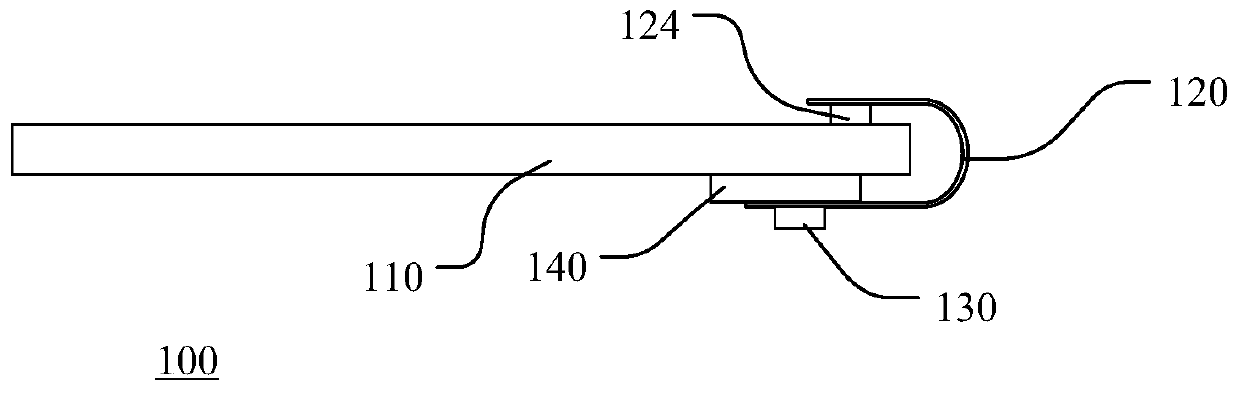
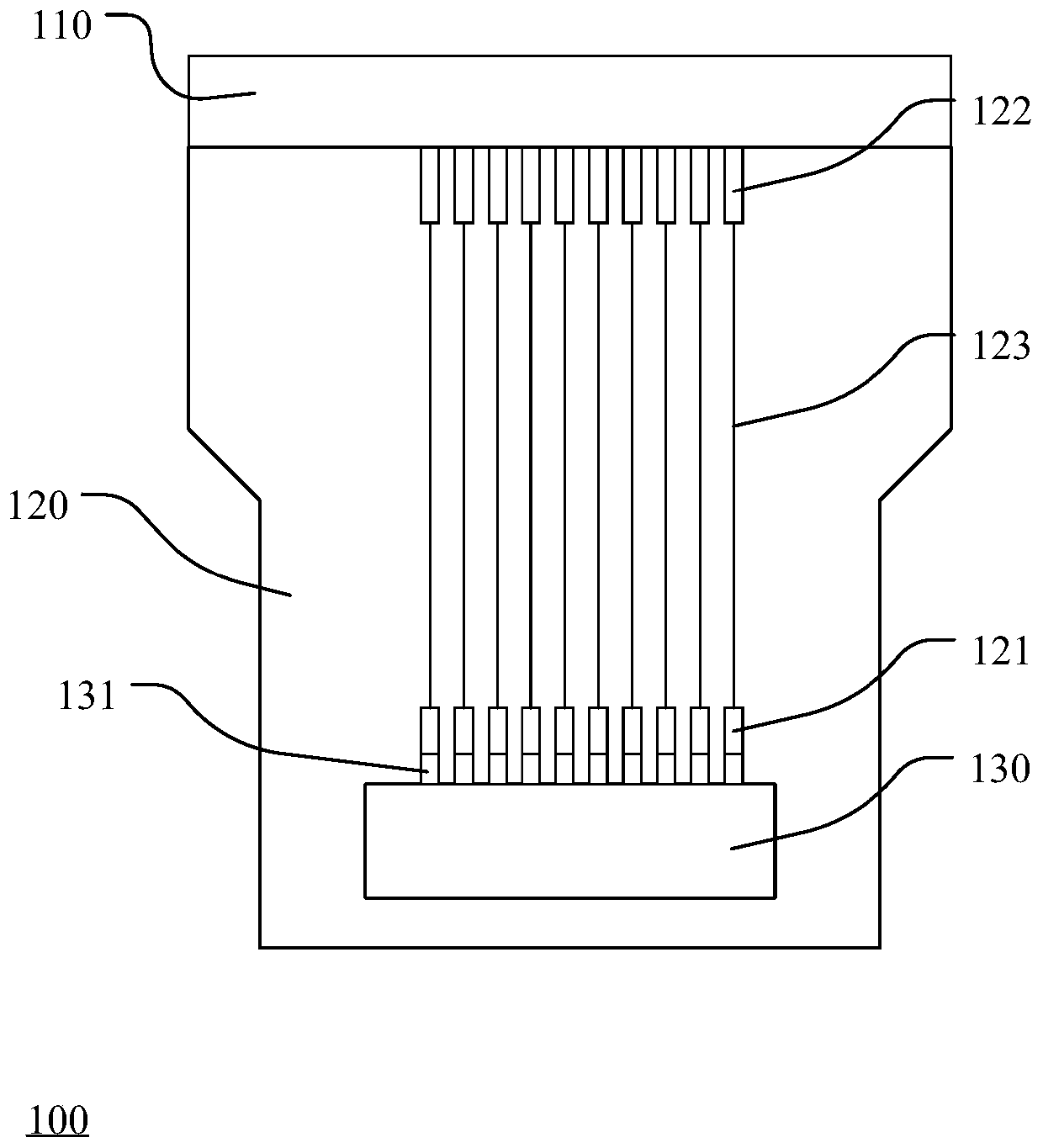
[0046] Figure 1a Shows an expanded view of a display device according to an embod...


PUM


Abstract

The invention discloses a display device, display system and manufacturing method. The display device comprises a display panel and a chip on film, wherein the chip on film comprises a driving chip, afirst electrode array, a second electrode array and a plurality of leads, the driving chip is provided with a plurality of chip pins; a plurality of chip pins are respectively led out by electrodes in the first electrode array; a second electrode array is used for providing a plurality of signal channels between the driving chip and the display panel; and the plurality of leads are respectively used for connecting the effective pins in the plurality of chip pins to the corresponding signal channels, so that the effective pins are electrically connected with the corresponding driving terminalson the display panel, when the plurality of chip pins comprise at least one idle pin and at least one effective pin, the leads, the effective pins and the driving terminals are the same in number. The chip of the display device comprises at least one idle pin, and the wiring density of the lead is reduced, so that the short circuit and electric leakage risks of the display device caused by overlarge wiring density are reduced, and the problem of increased coupling capacitance is avoided.

Description

Technical field [0001] The present invention relates to the field of display technology, and more specifically, to a display device, a display system and a manufacturing method. Background technique [0002] Liquid Crystal Display (LCD) and Organic Light-Emitting Diode (OLED) display devices have the advantages of stable picture, vivid image, elimination of radiation, space saving and energy saving, occupying the most important part of the flat display field. leading position. The display panel of the above-mentioned display device is provided with multiple scan lines and data lines, and the scan lines or data lines extend to the edge of the display panel to form leads for connecting with the driving chip. Due to the large number of scan lines and data lines, it is difficult to process with traditional soldering processes. Therefore, the chip on film (COF) packaging process is generally used to connect the display panel and the driving chip. [0003] The flip chip packaging proce...

Claims


Application Information

Patent Timeline
Patent Type & Authority Applications(China)
IPC IPC(8): G02F1/133G02F1/1345G02F1/1343
CPCG02F1/13306G02F1/134309G02F1/13452
Inventor 宫仁敏
Owner CHIPONE TECH BEIJINGCO LTD
Why Eureka
Try Eureka