Semiconductor structures and methods of forming them

A technology of semiconductors and fins, applied in the field of semiconductor structures and their formation, can solve the problems that the process methods of semiconductor structures need to be improved

Active Publication Date: 2022-02-15
SEMICON MFG INT (SHANGHAI) CORP +1
View PDF0 Cites 0 Cited by
  • Summary
  • Abstract
  • Description
  • Claims
  • Application Information

AI Technical Summary

Problems solved by technology

[0004] However, the process methods for forming semiconductor structures in the prior art still need to be improved

Method used


Image

  • Semiconductor structures and methods of forming them
  • Semiconductor structures and methods of forming them
  • Semiconductor structures and methods of forming them

Examples


Embodiment Construction

[0031] It can be seen from the background art that the process methods for forming semiconductor structures in the prior art still need to be improved.

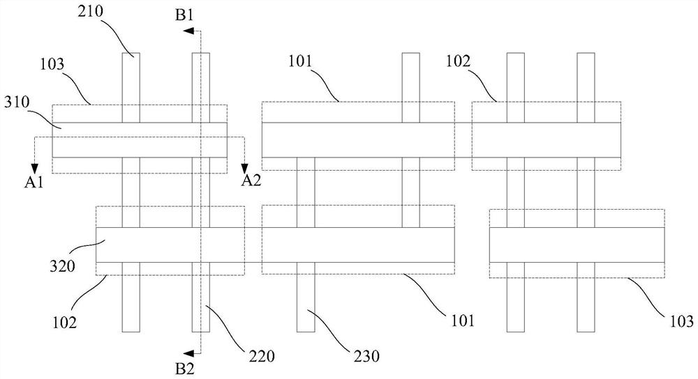
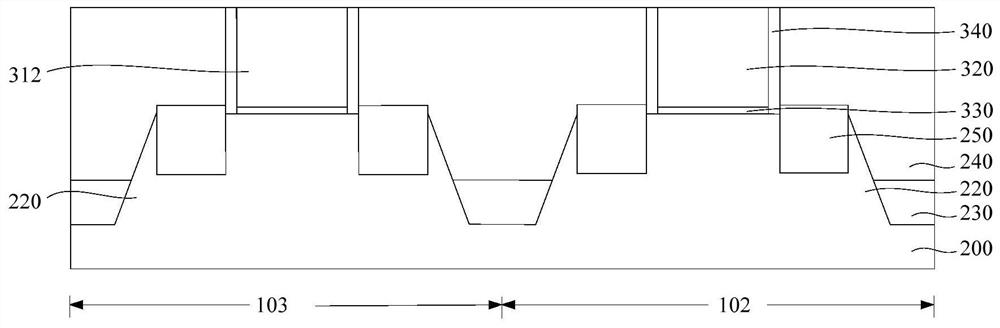
[0032] The reason for the analysis is that when multiple semiconductor structures are formed and the number of channel regions of the multiple semiconductor structures is different, the process methods for forming the multiple semiconductor structures are independent of each other, and each semiconductor structure is formed from the same Starting from the initial state, the process is cumbersome and the process time is long.

[0033] In order to solve the above problems, the present invention provides a method for forming a semiconductor structure, including: the number of fins is at least two, and the substrate exposed by the fins has an isolation layer, and the isolation layer has an part of the dummy gate; forming a dielectric layer on the isolation layer, the dielectric layer covering the sidewall of the dummy gate; remov...


PUM

PropertyMeasurementUnit
thicknessaaaaaaaaaa

Abstract

A semiconductor structure and its forming method, the forming method comprising: providing a substrate and fins protruding from the substrate, the number of the fins is at least two, and the fins are exposed on the substrate An isolation layer is provided, the isolation layer covers part of the sidewall of the fin, the isolation layer has a dummy gate across the fin, and the dummy gate covers part of the top and part of the sidewall of the fin; A dielectric layer is formed on the isolation layer, and the dielectric layer covers the sidewalls of the dummy gate; part of the dummy gate is removed to expose part of the tops of some number of fins, and a penetrating through the dielectric layer is formed in the dielectric layer. an opening in the layer thickness; forming an insulating layer that fills the opening. The present invention can form a semiconductor structure with a required number of channel regions on the basis of multiple positions where channel regions can be formed, thereby simplifying the process of forming a semiconductor structure with a specific number of channel regions.

Description

technical field [0001] The invention relates to the technical field of semiconductor manufacturing, in particular to a semiconductor structure and a forming method thereof. Background technique [0002] In semiconductor manufacturing, as the feature size of integrated circuits continues to decrease, the channel length of MOSFETs has also been shortened accordingly. However, as the channel length of the device is shortened, the distance between the source and the drain of the device is also shortened, resulting in poor control ability of the gate to the channel, and short-channel effects (SCE: short-channel effects) more likely to happen. [0003] The Fin Field Effect Transistor (FinFET) has outstanding performance in suppressing the short channel effect. The gate of the FinFET can control the fin at least from both sides. Therefore, compared with the planar MOSFET, the gate of the FinFET has an The control ability is stronger, and the short channel effect can be well suppr...

Claims


Application Information

Patent Timeline
Patent Type & Authority Patents(China)
IPC IPC(8): H01L29/06H01L21/336H01L29/78
CPCH01L29/785H01L29/66795H01L29/0642
Inventor 王楠
Owner SEMICON MFG INT (SHANGHAI) CORP
Why Eureka
Try Eureka