Film bulk acoustic wave resonator and manufacturing method thereof

A thin-film bulk acoustic wave and manufacturing method technology, applied in electrical components, impedance networks, etc., can solve problems such as unfavorable growth of single crystal piezoelectric materials, easy melting and damage of bottom electrodes, etc., to save manufacturing costs, not easy to melt and damage at high temperature, Yield-enhancing effect

Active Publication Date: 2019-08-09
SOUTH UNIVERSITY OF SCIENCE AND TECHNOLOGY OF CHINA
View PDF6 Cites 6 Cited by
  • Summary
  • Abstract
  • Description
  • Claims
  • Application Information

AI Technical Summary

Problems solved by technology

Single crystal piezoelectric materials are generally obtained by Metal Organic Chemical Vapor Deposition (MOCVD) under high temperature environment, but the laid bottom electrode is easily melted and damaged at high temperature, which is not conducive to the growth of single crystal piezoelectric materials.

Method used


Image

  • Film bulk acoustic wave resonator and manufacturing method thereof
  • Film bulk acoustic wave resonator and manufacturing method thereof
  • Film bulk acoustic wave resonator and manufacturing method thereof

Examples


Embodiment Construction

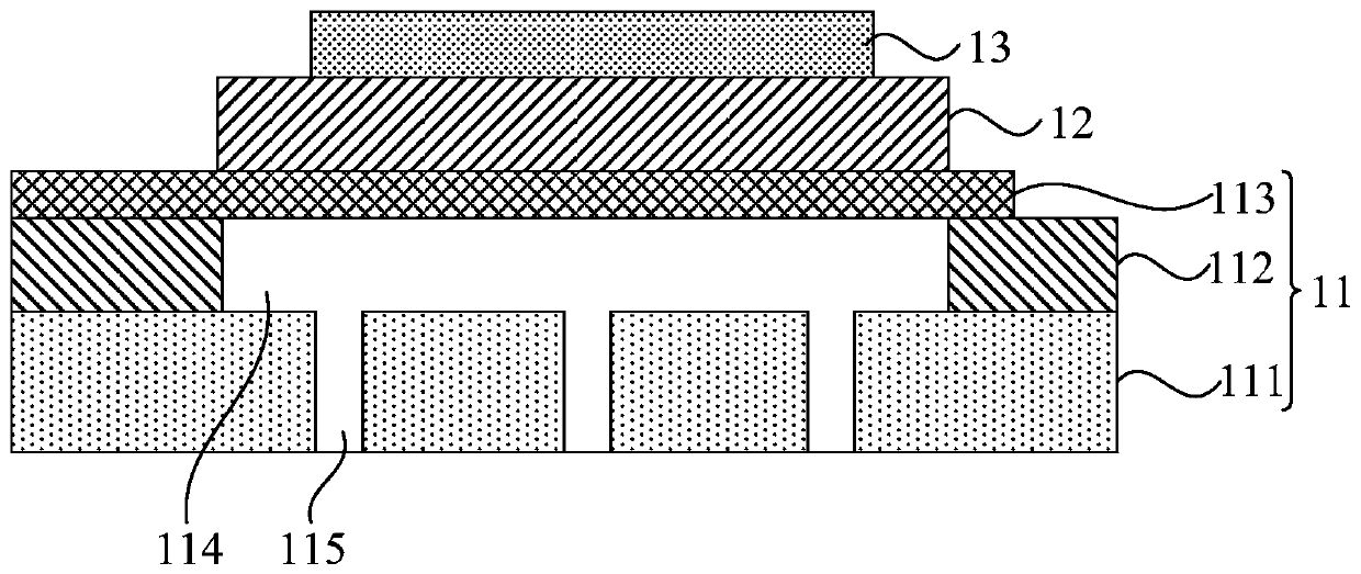
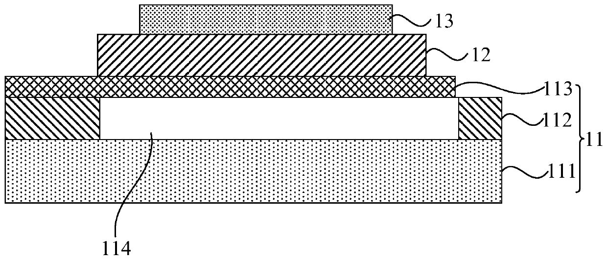
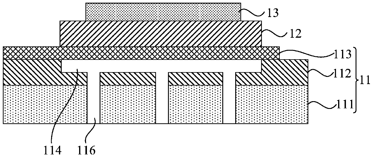
[0037] The present invention will be further described in detail below in conjunction with the accompanying drawings and embodiments. It should be understood that the specific embodiments described here are only used to explain the present invention, but not to limit the present invention. In addition, it should be noted that, for the convenience of description, only some structures related to the present invention are shown in the drawings but not all structures.

[0038] Thin film bulk acoustic resonator is widely used in wireless communication, and its core structure includes top electrode, piezoelectric film layer, and bottom electrode. In the traditional process, after the bottom electrode is formed, a piezoelectric thin film layer is deposited on the bottom electrode, and the material of the piezoelectric thin film layer can be a single crystal piezoelectric material or a polycrystalline piezoelectric material. Single crystal piezoelectric materials are superior to poly...


PUM


Abstract

The embodiment of the invention discloses a film bulk acoustic wave resonator and a manufacturing method thereof. The film bulk acoustic wave resonator comprises a silicon-on-insulator substrate; wherein the silicon-on-insulator substrate sequentially comprises a substrate, an insulating layer and a suspension silicon layer, the suspension silicon layer is doped with an impurity material, so thatthe suspension silicon layer is used as a bottom electrode; a piezoelectric film layer which is arranged on one side, far away from the substrate, of the suspension silicon layer; a top electrode which is arranged on one side, far away from the substrate, of the piezoelectric film layer; and an air cavity which is formed in one side, close to the suspension silicon layer, of the insulating layer.According to the technical scheme provided by the embodiment of the invention, an implementation scheme of the bottom electrode of the film bulk acoustic wave resonator can be provided, so that the problem that the bottom electrode is easy to damage is prevented.

Description

technical field [0001] Embodiments of the present invention relate to the technical field of wireless communication, and in particular to a thin-film bulk acoustic resonator and a manufacturing method thereof. Background technique [0002] With the rapid development of wireless communication, wireless signals are becoming more and more crowded, and new requirements such as integration, miniaturization, low power consumption, high performance, and low cost are put forward for filters working in the radio frequency band. Traditional surface acoustic wave filters are increasingly unable to meet such technical indicators due to limitations in frequency and power. Film Bulk Acoustic Resonator (FBAR) has gradually become a hot spot in the research of RF filters due to its characteristics of CMOS process compatibility, high quality factor, low loss, low temperature coefficient, and high power carrying capacity. [0003] The core structure of the film bulk acoustic resonator includ...

Claims


Application Information

Patent Timeline
Patent Type & Authority Applications(China)
IPC IPC(8): H03H3/02H03H9/02H03H9/17
CPCH03H3/02H03H9/02039H03H9/174H03H2003/023
Inventor 王亮程凯于洪宇
Owner SOUTH UNIVERSITY OF SCIENCE AND TECHNOLOGY OF CHINA
Why Eureka
Try Eureka