
Thick copper circuit board and manufacture method thereof

A technology of a thick copper circuit board and a manufacturing method, applied in the field of circuit board manufacturing, can solve the problems of gas residue, thick copper layer thickness of the thick copper circuit board, etc., and achieve the effect of avoiding dryply defects

Active Publication Date: 2019-08-06
广东依顿电子科技股份有限公司
View PDF20 Cites 7 Cited by
  • Summary
  • Abstract
  • Description
  • Claims
  • Application Information

AI Technical Summary

Problems solved by technology

[0012] The invention provides a thick copper circuit board, which solves the delamination problem caused by gas residue between the lines when the thick copper layer is thicker when the board is pressed.

Method used


Image

  • Thick copper circuit board and manufacture method thereof
  • Thick copper circuit board and manufacture method thereof
  • Thick copper circuit board and manufacture method thereof

Examples


Embodiment 1

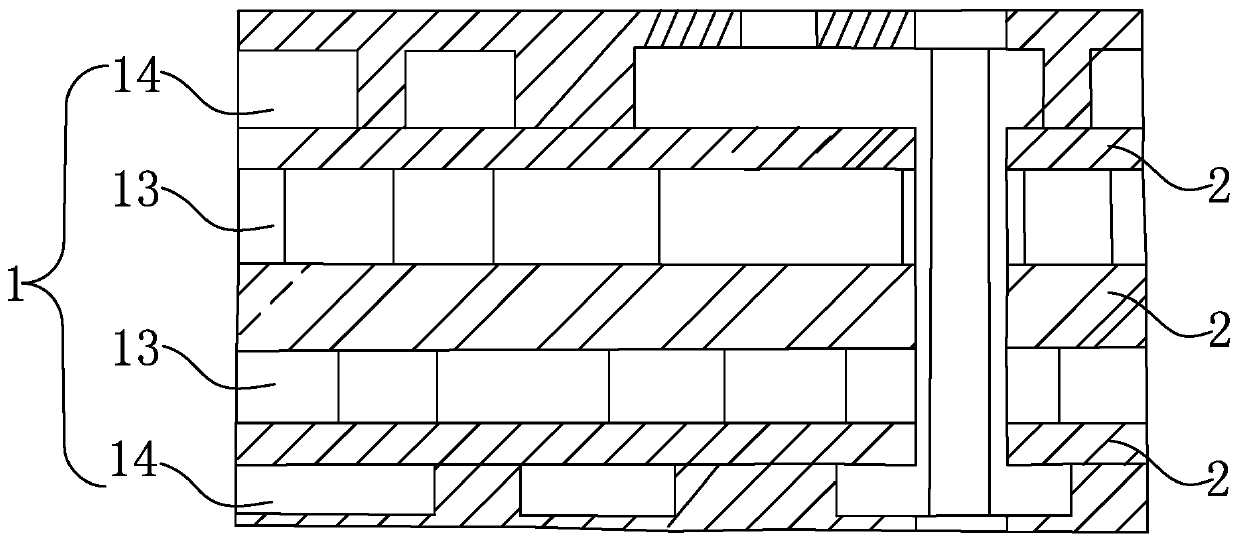
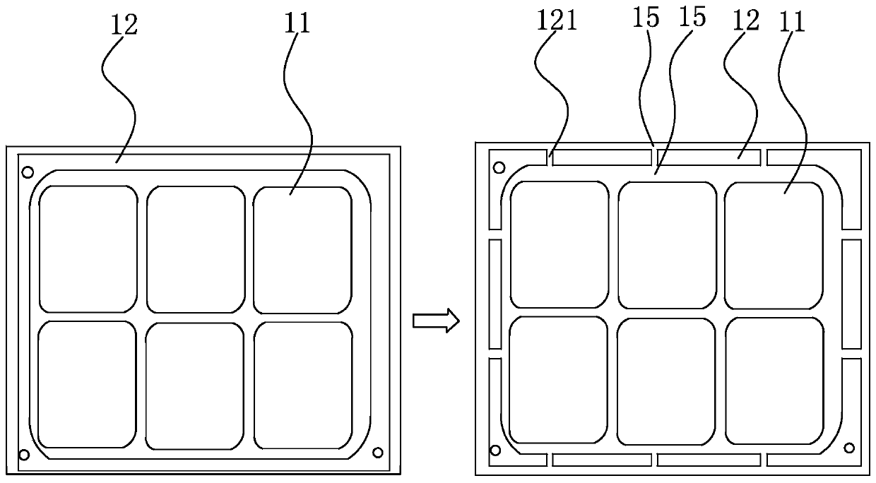
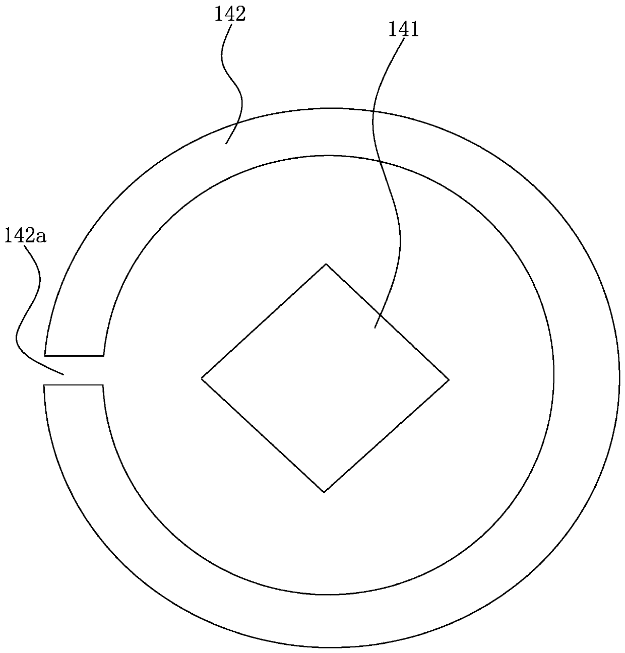
[0064] Example 1: See attached figure 1 to attach image 3 , the present embodiment provides a thick copper circuit board, including a multilayer graphic circuit layer 1 and a multilayer insulating dielectric layer 2, as attached figure 1 As shown, the insulating dielectric layer 2 is arranged between the two adjacent graphic circuit layers 1, and the insulating dielectric layer 2 is a prepreg, so as to isolate the two circuit layers and avoid the short circuit of the graphic circuit layer; The graphic circuit layer 1 is provided with at least one graphic circuit unit 11 , of course, a plurality of graphic circuit units may be provided as required, specifically designed according to the shape and size of the required graphic circuit unit. The edge of the graphic circuit layer is surrounded by a process edge 12, which is used to ensure the efficiency and quality of the thick copper circuit board in the subsequent assembly process, and can also disperse the heat received by the...

Embodiment 2

[0069] Example 2: See attached Figure 4 to attach Figure 5 , the present embodiment provides a method for manufacturing a thick copper circuit board, comprising the following steps:

[0070] S1. Material cutting: Cut the qualified thick copper clad laminate into a predetermined size and shape, and then clean and dry the surface. The thick copper clad laminate is made of cured resin film and 3OZ, 4OZ, 5OZ, 6OZ copper foil and other copper foils of the same or different thickness;

[0071] S2. Transfer of inner layer graphic circuit: a layer of photosensitive material is pasted on the copper clad core board, and then the negative graphic black film is used for counter-position exposure, so that the photosensitive material in the circuit area is cured during the exposure process, and the image is completed transfer. The black film is provided with graphic light blocking points, the shape and size of the graphic light blocking points are consistent with the shape and size of ...


PUM


Abstract

The invention discloses a thick copper circuit board and a manufacture method thereof. The thick copper circuit board comprises multiple graphic line layers and multiple insulating medium layers, eachinsulating medium layer is arranged between two adjacent graphic line layers, and includes a prepreg, each graphic line layer is internally provided with at least one graphic line unit, the edge of the graphic line layer is surrounded by a technical edge, and a gas guiding groove is formed in the technical edge, and penetrates internal and external sides of the technical edge. The guide guiding grooves are formed in the technical edges in the edges of the graphic line layers of the thick copper line layer, so that copper-free areas in the internal graphic line layers on the thick copper circuit board can be pumped into the vacuum state via the gas guiding grooves, it is ensured that the copper-free areas are fully filled with resin on the prepregs, and a dry ply defect is avoided.

Description

[0001] 【Technical field】 [0002] The invention relates to the technical field of circuit board manufacturing, in particular to a thick copper circuit board and a manufacturing method thereof. [0003] 【Background technique】 [0004] With the rapid development of electronics and power communication technology, some high-current and high-power power supply products are more and more widely used, and the number of functional components integrated on the circuit board is increasing. The requirements are getting higher and higher, and the copper thickness of the circuit board will become thicker and thicker. The circuit board industry usually refers to the circuit board with a bottom copper thickness of 105 μm (3OZ) and above as a thick copper circuit board. Thick copper circuit board has the characteristics of strong conduction capacity, high reliability and high heat dissipation performance. It is suitable for the current rapid development of new energy electric vehicles and elec...

Claims


Application Information

Patent Timeline
IPC IPC(8): H05K1/02H05K3/00H05K3/06H05K3/46H05K3/42
CPCH05K1/0298H05K1/0269H05K3/0052H05K3/06H05K3/4611H05K3/42H05K3/423
Inventor 莫介云
Owner 广东依顿电子科技股份有限公司
Learn More