
Asymmetric MZI optical waveguide temperature sensor based on loaded strip-shaped structure and preparation method thereof

A technology of temperature sensor and strip waveguide, which is applied in the field of asymmetric MZI optical waveguide temperature sensor based on loaded strip structure and its preparation, can solve the problems of limiting the practical application of temperature sensor and the inability to realize the temperature monitoring function, etc. Large-scale production, exacerbating the change of output light intensity, and the effect of process compatibility

Inactive Publication Date: 2019-08-02
JILIN UNIV
View PDF9 Cites 2 Cited by
  • Summary
  • Abstract
  • Description
  • Claims
  • Application Information

AI Technical Summary

Problems solved by technology

However, in practical applications, the two interference arms of MZI are in the same environment at the same time, and the effective refractive index changes of the two interference arms are the same, so that the monitoring function of temperature cannot be realized. Practical application of temperature sensor with waveguide structure

Method used


Image

  • Asymmetric MZI optical waveguide temperature sensor based on loaded strip-shaped structure and preparation method thereof
  • Asymmetric MZI optical waveguide temperature sensor based on loaded strip-shaped structure and preparation method thereof
  • Asymmetric MZI optical waveguide temperature sensor based on loaded strip-shaped structure and preparation method thereof

Examples


Embodiment Construction

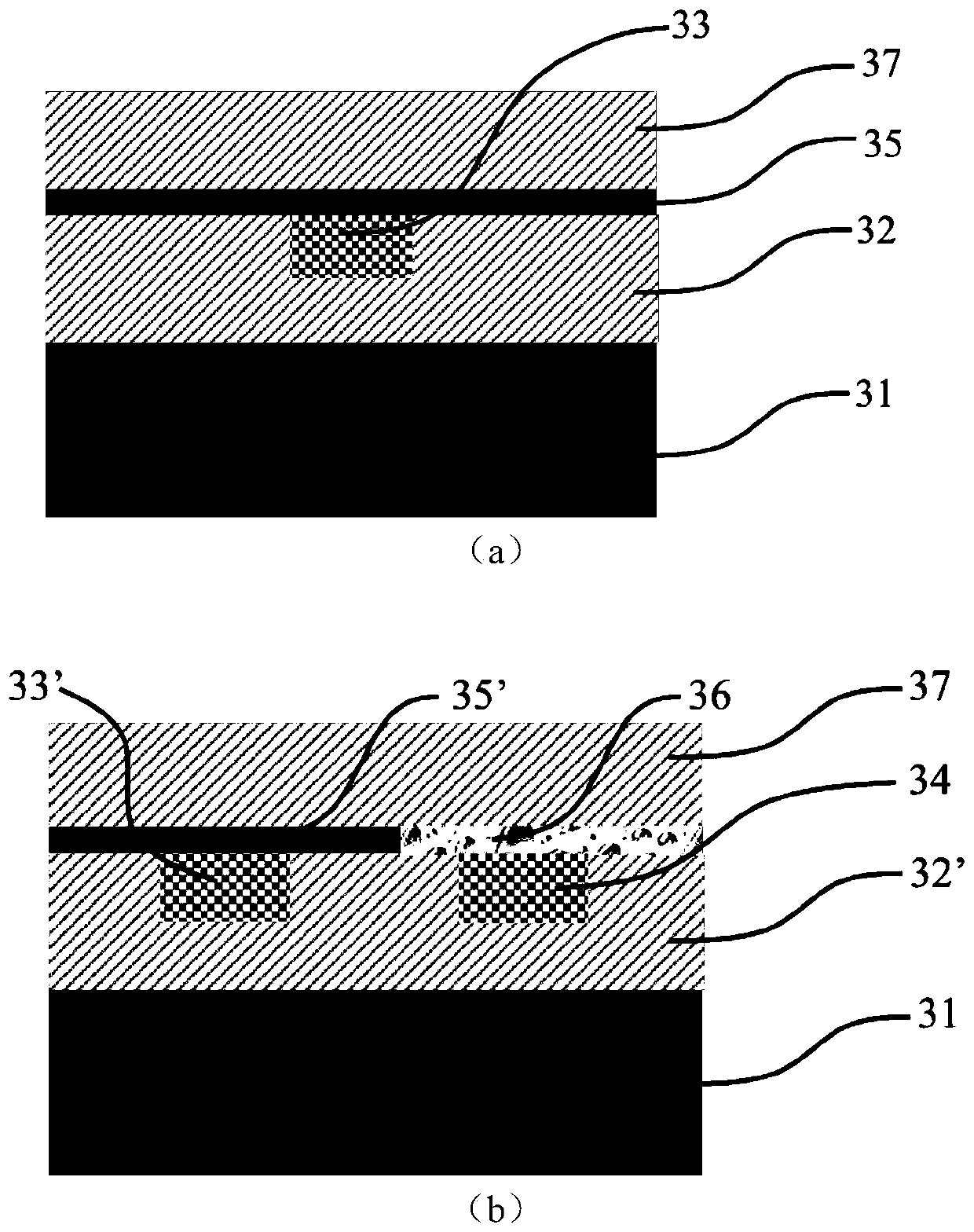
[0046] Cleaning treatment of silicon substrate: Soak the silicon substrate in acetone solution and ultrasonically clean it for 8 minutes, then wipe it repeatedly with acetone and ethanol cotton balls successively, rinse it with deionized water, blow dry it with nitrogen, and finally put it under the condition of 100℃ Bake for 1 hour to remove moisture.

[0047] The lower cladding of the polymer waveguide was prepared by spin-coating: the polymer material PMMA was spin-coated on the cleaned silicon wafer substrate, the spin-coating speed was controlled at 4000 rpm, and then the film was baked at 120°C for 2 hours , to obtain a waveguide lower cladding with a thickness of 6 μm.

[0048] The waveguide groove was prepared by standard photolithography and dry etching process: first, a layer of Al mask with a thickness of 100nm was evaporated on the prepared polymer lower cladding layer, and the Al film was spin-coated by spin-coating process. A layer of positive photoresist BP212 ...


PUM

PropertyMeasurementUnit
Thicknessaaaaaaaaaa
Thicknessaaaaaaaaaa
Thicknessaaaaaaaaaa

Abstract

The invention, which belongs to the technical field of a planar optical waveguide sensor and preparation thereof, provides an asymmetric MZI optical waveguide temperature sensor based on a loaded strip-shaped structure and a preparation method thereof. The asymmetric MZI optical waveguide temperature sensor comprises an input straight waveguide, a 3-dB Y-branch beam splitter, two asymmetric reference arm and sensing arm, a 3-dB Y-branch coupler and an output straight waveguide. The reference arm and the sensing arm include silicon substrates, lower polymer claddings with double-waveguide groove structures, reference arm optical waveguide core layers and sensing arm optical waveguide core layers, and unexposed and exposed organic-inorganic hybrid material flat plates, and upper polymer claddings that are arranged successively from bottom to top. According to the invention, with the organic-inorganic hybrid materials containing the chromophore molecules on the surface of the photo-bleaching sensor arm, the refractive index changes, the difference of the optical mode field with the environment change in light transmission of two interference arms is increased further, and the output light intensity change is increased. Therefore, the sensor has an important practical application value.

Description

technical field [0001] The invention belongs to the technical field of planar optical waveguide sensors and their preparation, and specifically relates to a waveguide core layer with a silicon chip as a substrate, an organic-inorganic hybrid material as a loaded strip waveguide, and an organic polymer with a large thermo-optic coefficient. and cladding asymmetric Mach–Zehnder interferometer (MZI) optical waveguide temperature sensor and its preparation method. Background technique [0002] Temperature is closely related to the environment in which human beings live. People's daily life, agricultural product planting, animal reproduction, scientific research and many other fields are all closely related to temperature measurement. Therefore, the precise measurement of temperature has been an important research direction for a long time. With the development of science and technology, the monitoring of temperature is developing in the direction of high precision, large resolu...

Claims


Application Information

Patent Timeline
IPC IPC(8): G01K11/32
CPCG01K11/32
Inventor 张大明牛东海王希斌许强姜明慧王力磊
Owner JILIN UNIV
Learn More