A processing method and processing system for a circuit board

A processing method and circuit board technology, which is applied in the field of circuit board processing, can solve problems such as warping and deformation of surfaces or points near cutting, and achieve the effects of narrow line spacing, simple process, and low cost

Active Publication Date: 2022-04-05
奈米科技(深圳)有限公司
View PDF6 Cites 0 Cited by
  • Summary
  • Abstract
  • Description
  • Claims
  • Application Information

AI Technical Summary

Problems solved by technology

[0006] The technical problem to be solved by the present invention is to provide a bonding-assisted laser cutting circuit board process, which overcomes the above-mentioned defects of the prior art, such as solving the warping or deformation of the surface or point near the cutting caused by the heat of the copper foil during cutting. problems, and effectively maintain the accuracy of laser cutting patterns

Method used


Image

  • A processing method and processing system for a circuit board
  • A processing method and processing system for a circuit board
  • A processing method and processing system for a circuit board

Examples


Embodiment Construction

[0046] Now in conjunction with the accompanying drawings, the preferred embodiments of the present invention will be described in detail.

[0047] Such as figure 1 As shown, the present invention provides a preferred embodiment of a circuit board processing method.

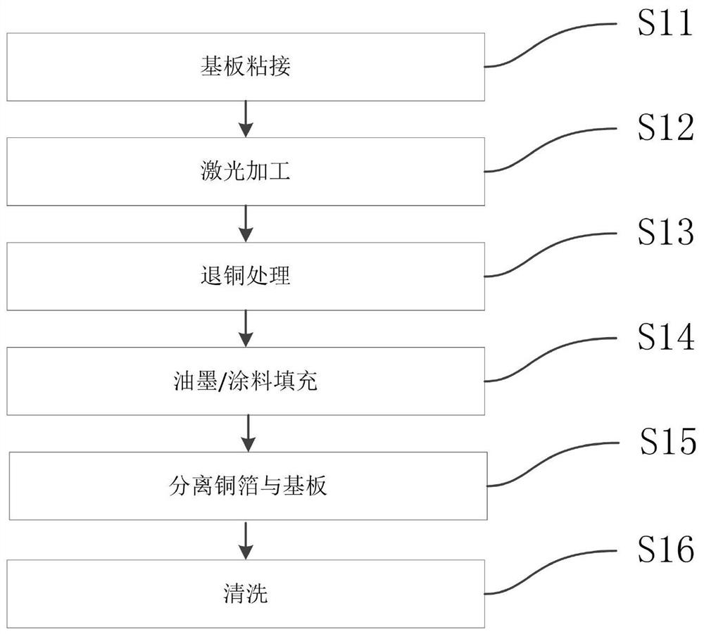
[0048] A processing method for a circuit board, the steps of the processing method comprising:

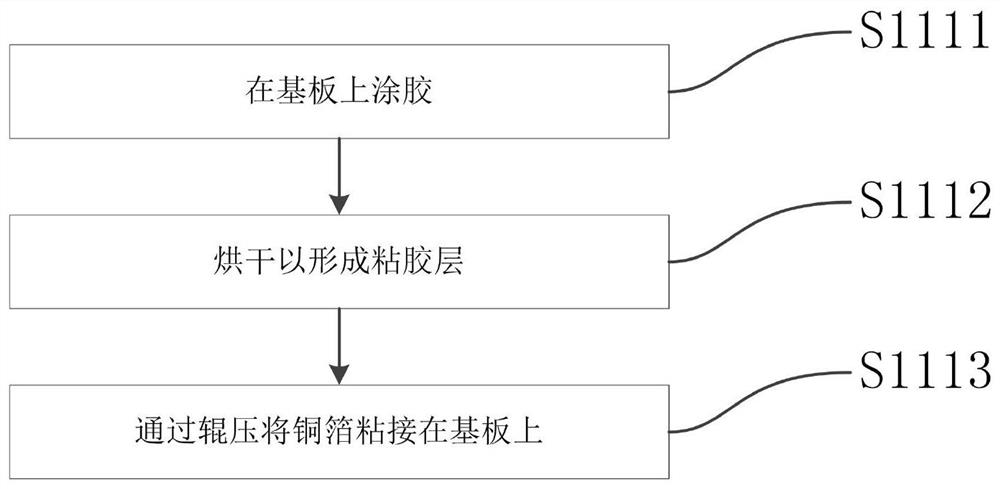
[0049] Step S11, bonding the substrate, setting a copper foil on the substrate through the adhesive layer;

[0050] Step S12, laser processing, laser cutting the copper foil according to the preset circuit diagram to obtain the first semi-finished circuit board;

[0051] Step S13, copper stripping treatment to obtain the second semi-finished circuit board;

[0052] Step S14, filling with ink or paint, using ink or paint to fill the laser-cut gap, and forming a layer of ink / paint on the surface of the copper foil to obtain a third semi-finished circuit board;

[0053] Step S15, separating the copper foil and the sub...


PUM


Abstract

The invention relates to the technical field of laser processing, in particular to a processing method and a processing system for a circuit board. The steps of the processing method include: substrate bonding, setting a copper foil on the substrate through an adhesive layer; laser processing; copper stripping treatment; ink or paint filling; separating the copper foil and the substrate; cleaning to obtain a finished circuit board. The invention can effectively prevent warping or deformation of the copper foil after being heated during laser cutting by bonding the copper foil on the substrate, thereby removing the error influence caused by it on the cutting line and depth. At the same time, it can A product with narrower line spacing is obtained; further, after obtaining the cutting pattern, use insulating fillers such as ink to fill the cut groove, further protect and fix the pattern, and obtain a more accurate pattern, and the process is simple, low in cost, and convenient for large-scale scale production needs.

Description

technical field [0001] The invention relates to the technical field of circuit board processing, in particular to a circuit board processing method and a processing system. Background technique [0002] Laser processing technology is a processing technology that uses the characteristics of the interaction between laser beams and substances to perform cutting, welding, surface treatment, drilling and micro-processing of materials (including metals and non-metals). [0003] Laser cutting of circuit boards uses the high-energy and strong beam of the laser to achieve instantaneous high temperature in the area scanned by the laser through photothermal conversion to vaporize the copper foil. [0004] In the prior art, when the laser cuts the circuit board, if the copper foil is not on a fixed surface, the laser processing will cause deformation and warping of the copper foil under the condition of high heat dissipation, thereby changing the height of the copper foil processing sur...

Claims


Application Information

Patent Timeline
Patent Type & Authority Patents(China)
IPC IPC(8): H05K3/02
CPCH05K3/027H05K2203/0528
Inventor 夏丽红
Owner 奈米科技(深圳)有限公司
Why Eureka
Try Eureka