PCB assembly, manufacturing method of PCB assembly and electronic device

A manufacturing method and technology for electronic equipment, which are applied in the manufacture of printed circuits, assembling printed circuits with electrical components, and printed circuits, etc., can solve problems such as warping of the upper board, poor performance of PCB components, and reduced product yield of PCB components. , to achieve the effect of improving comprehensive practical performance, improving product yield, and enhancing market competitiveness

Active Publication Date: 2021-04-30
OPPO CHONGQING INTELLIGENT TECH CO LTD
View PDF7 Cites 0 Cited by
  • Summary
  • Abstract
  • Description
  • Claims
  • Application Information

AI Technical Summary

Problems solved by technology

Due to the thin thickness of the upper layer board (the PCB board on the top layer), when the upper layer board and the interlayer board (the PCB board in the middle position) are welded and connected, the upper layer board is easily warped due to heat, which will cause the upper layer board to appear False soldering causes poor performance of PCB components, which greatly reduces the product yield of PCB components

Method used


Image

  • PCB assembly, manufacturing method of PCB assembly and electronic device
  • PCB assembly, manufacturing method of PCB assembly and electronic device
  • PCB assembly, manufacturing method of PCB assembly and electronic device

Examples


Embodiment Construction

[0027] Embodiments of the present application are described in detail below, examples of which are shown in the drawings, wherein the same or similar reference numerals denote the same or similar elements or elements having the same or similar functions throughout. The embodiments described below by referring to the figures are exemplary, and are only for explaining the present application, and should not be construed as limiting the present application.

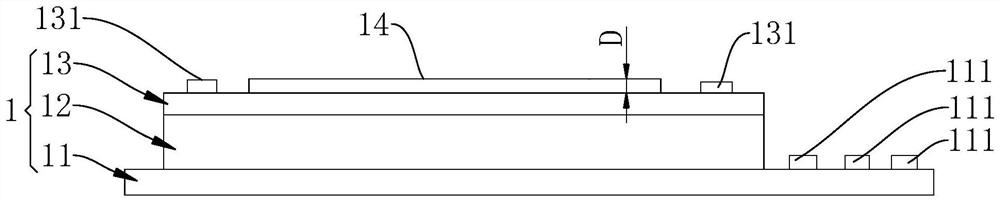
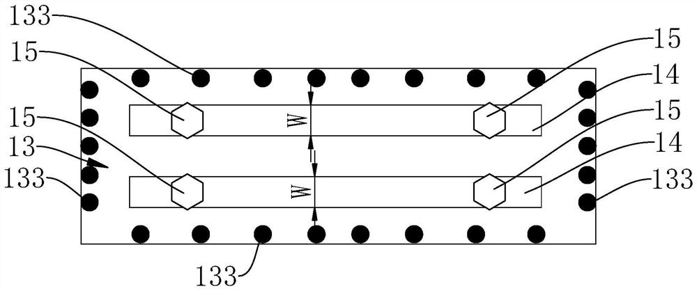
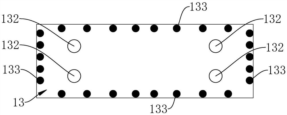
[0028] Refer below Figure 1-Figure 3 A PCB (Printed Circuit Board, printed circuit board) assembly according to an embodiment of the present application is described, including: a bottom main board 11 , an upper board 13 and at least one interlayer board 12 .

[0029] Such as figure 1 As shown, the bottom main board 11 can be provided with a first electronic component 111, the interlayer board 12 can be arranged between the bottom main board 11 and the upper board 13, the bottom main board 11 and the upper board 13 can be ...


PUM


Abstract

The application discloses a PCB assembly, a manufacturing method of the PCB assembly and electronic equipment. The PCB assembly includes: a bottom main board, an upper board and at least one interlayer board. The bottom main board is provided with a first electronic component, the upper plate is provided with a second electronic component and a fixing plate for avoiding the installation of the second electronic component, the fixing plate is used to support the upper plate to prevent the upper plate from warping due to heat, and the sandwich plate It is arranged between the bottom main board and the upper board, and the bottom main board and the upper board are electrically connected through the interlayer board. According to the PCB assembly of the present application, by arranging the fixing plate on the upper layer, the fixing plate can fix and support the upper layer and prevent the upper layer from warping due to heat. As a result, it can not only prevent the deformation of the overall structure of the PCB assembly, but also prevent the phenomenon of virtual welding between the upper board and the interlayer board, which can form a stable electrical connection between the upper board and the bottom board, and greatly improve the quality of the PCB assembly. product yield.

Description

technical field [0001] The present application relates to the field of printed circuit boards, in particular to a PCB assembly, a method for manufacturing the PCB assembly, and electronic equipment. Background technique [0002] In the related art, a PCB assembly having multiple layers of PCB boards is provided in the electronic equipment. Due to the thin thickness of the upper board (the PCB board on the top layer), when the upper board and the interlayer board (the PCB board in the middle position) are welded and connected, the upper board is easily warped due to heat, which will cause the upper board to appear False soldering causes poor performance of PCB components, which greatly reduces the product yield of PCB components. Contents of the invention [0003] This application aims to solve at least one of the technical problems existing in the prior art. Therefore, an object of the present application is to provide a PCB assembly, which has the advantages of good sol...

Claims


Application Information

Patent Timeline
Patent Type & Authority Patents(China)
IPC IPC(8): H05K1/14H05K3/36
CPCH05K1/144H05K3/368
Inventor 杨鑫
Owner OPPO CHONGQING INTELLIGENT TECH CO LTD
Why Eureka
Try Eureka