Gallium oxide field effect transistor using stannous oxide to adjust threshold voltage and preparation method

A stannous oxide and gallium oxide field technology, applied in circuits, transistors, electrical components, etc., can solve the problem of large threshold voltage of field effect transistors, and achieve the effect of improving the utilization value

Pending Publication Date: 2019-07-19
山东大学深圳研究院 +1
View PDF8 Cites 3 Cited by
  • Summary
  • Abstract
  • Description
  • Claims
  • Application Information

AI Technical Summary

Problems solved by technology

[0006] Aiming at the problem that the uncertainty of the thickness of the stripped gallium oxide film leads to a large threshold voltage of the field effect transistor, and the device needs a large negative voltage to turn off the problem, we use the stripping method to obtain a high-quality gallium oxide film to prepare a field effect transistor, and use p-type SnO and n-type gallium oxide form a p-n junction to adjust the threshold voltage of gallium oxide field effect transistors, realizing a large positive shift of the threshold voltage, and further meeting its practical application requirements in power devices

Method used


Image

  • Gallium oxide field effect transistor using stannous oxide to adjust threshold voltage and preparation method
  • Gallium oxide field effect transistor using stannous oxide to adjust threshold voltage and preparation method
  • Gallium oxide field effect transistor using stannous oxide to adjust threshold voltage and preparation method

Examples


Embodiment 1

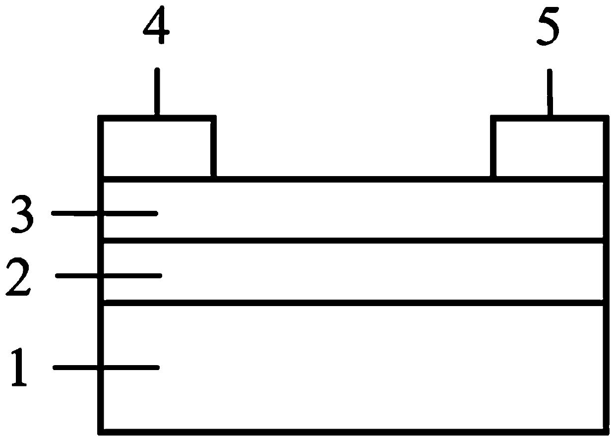
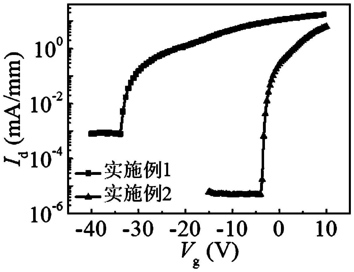
[0030] Embodiment 1, embodiment 1 is not provided with the gallium oxide field effect transistor of tin oxide layer, and it is used as contrast, as figure 1 As shown, a schematic diagram of its structure is given, and the structure is as follows figure 1 As shown, a bottom gate dielectric layer 2 and a gallium oxide channel layer 3 are sequentially arranged on a substrate 1 from bottom to top, and a source electrode 4 and a drain electrode 5 are arranged on the gallium oxide channel layer 3 .

[0031] The substrate is a silicon substrate, and the bottom gate is silicon. The thickness of the bottom gate dielectric layer is 100 nm, and the bottom gate dielectric layer is silicon oxide. The gallium oxide channel layer uses gallium oxide film as the channel layer, the thickness of the gallium oxide film is 185 nm, and it is n-type doped gallium oxide with a doping concentration of 5 × 10 16 cm -3 - 5 x 10 18 cm -3 . The source electrode is Ti / Au laminated metal, the thick...

Embodiment 2

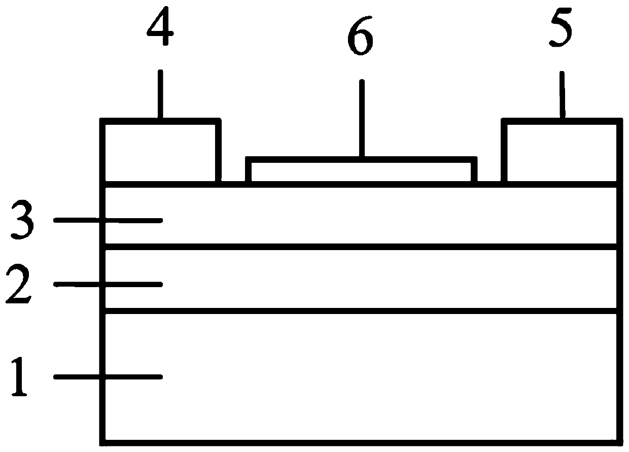
[0039] Example 2, such as figure 2 As shown, the structure schematic diagram of the gallium oxide field effect transistor of the present invention is provided with the tin oxide layer, which is composed of the substrate and the bottom gate electrode 1, the bottom gate dielectric layer 2, the gallium oxide channel layer 3, the source electrode 4 , a drain electrode 5 and a SnO layer 6, the substrate and the bottom gate electrode 1 can be used as the substrate and the gate electrode at the same time, the bottom gate dielectric layer 2 is arranged on the upper surface of the substrate, and the gallium oxide channel layer 3 is arranged on the On the bottom gate dielectric layer 2, the source electrode 4 and the drain electrode 5 are arranged on the upper surface of the gallium oxide channel layer 3, and the tin oxide layer 6 is arranged on the gallium oxide channel layer 3 between the source electrode 4 and the drain electrode 5 , and the SnO layer 6 is not in contact with the so...


PUM


Abstract

The invention discloses a gallium oxide field effect transistor using stannous oxide to adjust a threshold voltage. The gallium oxide field effect transistor comprises a substrate, a gate electrode, asource electrode and a drain electrode; a bottom gate dielectric layer is arranged on the upper surface of the substrate; a gallium oxide channel layer is arranged on the bottom gate dielectric layer, and the gallium oxide channel layer is made of N-type doped gallium oxide; and a stannous oxide layer is arranged on the gallium oxide channel layer between the source electrode and the drain electrode. The preparation method of the field effect transistor comprises the following steps that a) the substrate is cleaned; b) a gallium oxide thin film is prepared; c) a transfer object is removed; d)the source electrode and the drain electrode are prepared; e) the stannous oxide layer is prepared; and f) annealing treatment is carried out. The method aims to solve the problem that an existing gallium oxide transistor can be turned off only by a very high negative voltage, and provides a method and a process for adjusting the threshold voltage of the n-type gallium oxide field effect transistor by utilizing p-type stannous oxide, so that the threshold voltage of the transistor can be regulated, the threshold voltage of the device can be obviously improved, and the utilization value of thedevice can be improved.

Description

technical field [0001] The invention relates to a gallium oxide field-effect transistor and a preparation method thereof, and more specifically relates to a gallium oxide field-effect transistor and a preparation method thereof which use stannous oxide to adjust threshold voltage, and belongs to the technical field of semiconductor devices. Background technique [0002] Gallium oxide is a new type of fourth-generation direct bandgap wide-bandgap semiconductor. Compared with the third-generation semiconductor, it has outstanding advantages such as larger bandgap width, shorter absorption cut-off edge, and lower growth cost. It has become a power One of the preferred materials for devices and deep ultraviolet optoelectronic devices. However, conventional gallium oxide field effect transistors have a high threshold voltage and are depletion-mode transistors that require a large negative voltage to turn off. [0003] Gallium oxide thin films can be grown by chemical vapor depos...

Claims


Application Information

Patent Timeline
Patent Type & Authority Applications(China)
IPC IPC(8): H01L29/786H01L21/34
CPCH01L29/7869H01L29/66969
Inventor 辛倩刘雅璇宋爱民徐明升杜路路
Owner 山东大学深圳研究院
Why Eureka
Try Eureka