
Optical proximity correction method and mask making method

A technology of optical proximity correction and exposure conditions, which is applied in the direction of optics, originals for photomechanical processing, and photoplate-making processes on patterned surfaces, and can solve problems such as small process windows

Active Publication Date: 2022-04-15
SEMICON MFG INT (SHANGHAI) CORP +1
View PDF5 Cites 0 Cited by
  • Summary
  • Abstract
  • Description
  • Claims
  • Application Information

AI Technical Summary

Problems solved by technology

[0005] However, the process window of the optical proximity corrected pattern in the prior art is small

Method used


Image

  • Optical proximity correction method and mask making method
  • Optical proximity correction method and mask making method
  • Optical proximity correction method and mask making method

Examples


Embodiment Construction

[0022] As mentioned in the background, the process window of the graphics obtained by the existing optical proximity correction method is relatively small.

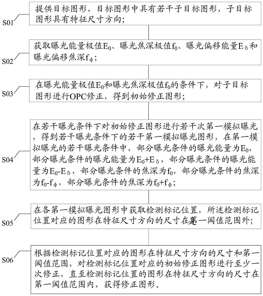
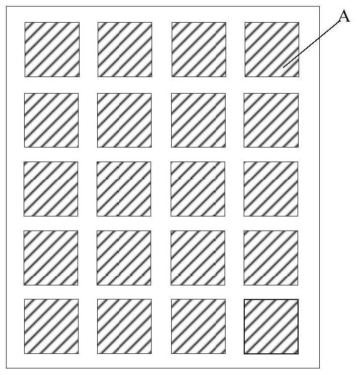
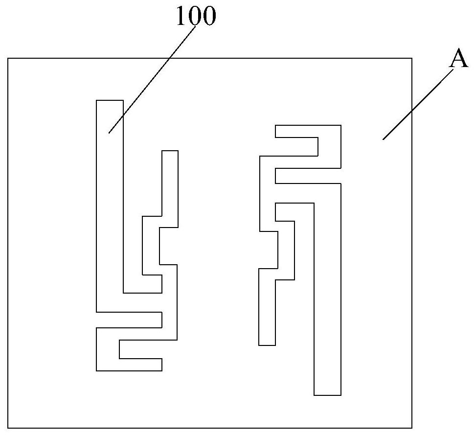
[0023] An optical proximity correction method, comprising: providing a target figure, in which there are several sub-target figures; setting the exposure energy extremum E 0 and exposure depth of focus extremum f 0 ;Provide OPC correction model; at the extreme value of exposure energy E0 and exposure depth of focus extremum f 0 Under the condition of , OPC correction is performed on the sub-object figure according to the OPC correction model to obtain a corrected figure, and the edge placement error of the corrected figure is less than or equal to the first threshold.

[0024] After the corrected figure is obtained, it is usually necessary to perform OPC detection on the corrected figure to obtain the position of the detection mark, which is usually called a weak point. Specifically, the simulated exposure is performed ...


PUM


Abstract

An optical proximity correction method and a method for making a mask plate. The correction method includes: performing OPC correction on a sub-target figure to obtain an initial correction figure; performing several first simulation exposures on the initial correction figure to obtain a number of The first simulated exposure pattern; obtain the detection mark position in each first simulated exposure pattern, the size of the figure corresponding to the detection mark position in the direction of the feature size is outside the first threshold range; according to the figure corresponding to the detection mark position in the feature size The size of the direction and the first threshold range are corrected at least once on the initial correction figure corresponding to the position of the detection mark to obtain the correction figure. The crafting window for correction graphics has been increased.

Description

technical field [0001] The invention relates to the field of semiconductor manufacturing, in particular to an optical proximity correction method and a mask plate manufacturing method. Background technique [0002] Photolithography technology is a crucial technology in semiconductor manufacturing technology. Photolithography technology can realize the transfer of graphics from the mask to the surface of the silicon wafer to form semiconductor products that meet the design requirements. The photolithography process includes an exposure step, a development step performed after the exposure step, and an etching step after the development step. In the exposure step, light is irradiated onto the silicon wafer coated with photoresist through the light-transmitting area of ​​the mask, and the photoresist reacts chemically under the irradiation of light; The photoresist is different to the degree of dissolution of the developer, forming a photoresist pattern, and realizing the tran...

Claims


Application Information

Patent Timeline
Patent Type & Authority Patents(China)
IPC IPC(8): G03F1/36
CPCG03F1/36
Inventor 闵金华李艳丽郝静安沈泫
Owner SEMICON MFG INT (SHANGHAI) CORP
Learn More