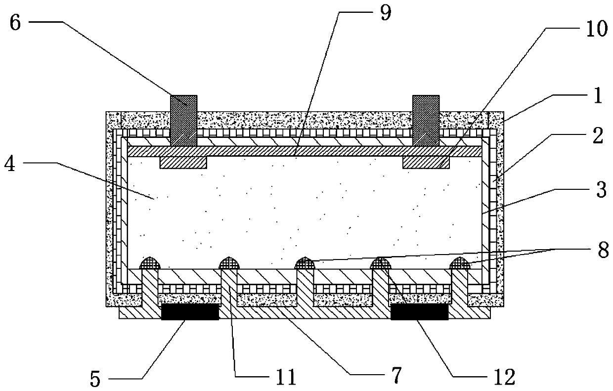
Three-layer dielectric passivation film PERC solar cell and manufacturing process
A technology of solar cells and passivation films, applied in the field of solar photovoltaic power generation, can solve the problems of poor passivation effect of PERC cells, increase the short-circuit current and open-circuit voltage of the battery, etc., so as to enhance the comprehensive utilization rate, increase the short-circuit current and open-circuit voltage, etc. , the effect of good density
- Summary
- Abstract
- Description
- Claims
- Application Information
AI Technical Summary
Problems solved by technology
Method used
Image
Examples
Embodiment 1
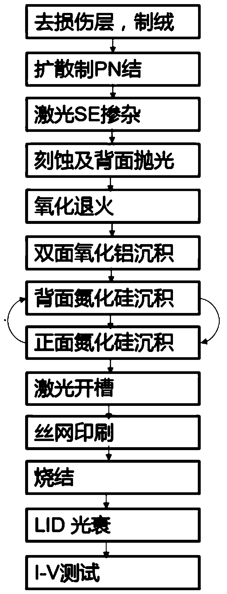
[0060] The present invention comprises the following concrete steps:
[0061] (1) Remove the mechanical damage layer 4um on the surface of the single crystal p-type silicon wafer with a NaOH solution with a concentration of 40g / L, clean the surface of the silicon wafer, and simultaneously etch the surface of the silicon wafer anisotropically with 18g / L of NaOH liquid, Form 2~3um inverted pyramid suede texture;
[0062] (2) Using POCl 3 The negative pressure of the liquid source diffuses the silicon wafer cleaned in step (1) in the diffusion furnace tube to form a P-N junction. The diffusion temperature is 830°C, the process time is 55 minutes, and the diffusion sheet resistance is controlled at 130-150Ω / □;
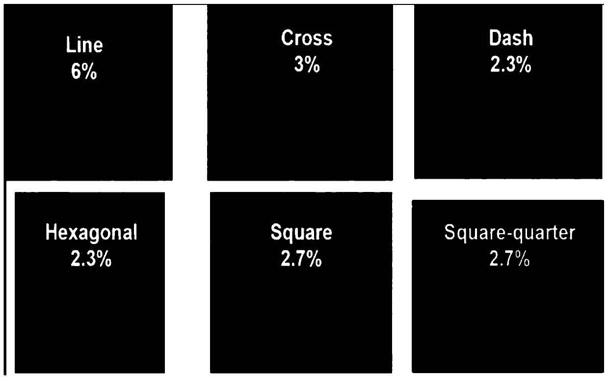
[0063] (3) Laser SE doping: On the silicon wafer diffused in step (2), the phosphorous atoms on the diffused surface phosphosilicate glass are laser doped in the subsequent screen-printed main grid and fine grid electrode regions by laser. The area of this area account...
Embodiment 2
[0076] The present invention comprises the following concrete steps:
[0077] (1) Use a NaOH solution with a concentration of 30g / L to remove the 3.5um mechanical damage layer on the surface of the single crystal p-type silicon wafer, clean the surface of the silicon wafer, and at the same time use 20g / L NaOH liquid to anisotropize the surface of the silicon wafer Corrosion, forming 3~4um inverted pyramid suede texture;
[0078] (2) Using POCl 3 The liquid source negative pressure diffuses the silicon wafer cleaned in step (1) in the diffusion furnace tube to form a P-N junction, the diffusion temperature: 850°C, the process time: 45min, and the diffusion sheet resistance is controlled at 140-170Ω / □;
[0079] (3) Laser SE doping: On the silicon wafer diffused in step (2), the phosphorous atoms on the diffused surface phosphosilicate glass are laser doped in the subsequent screen-printed main grid and fine grid electrode regions by laser. The area of this area accounts for ...
PUM
| Property | Measurement | Unit |
|---|---|---|
| Film thickness | aaaaa | aaaaa |
| Film thickness | aaaaa | aaaaa |
| Thickness | aaaaa | aaaaa |
Abstract
Description
Claims
Application Information
 - R&D Engineer
- R&D Manager
- IP Professional
- Industry Leading Data Capabilities
- Powerful AI technology
- Patent DNA Extraction
Browse by: Latest US Patents, China's latest patents, Technical Efficacy Thesaurus, Application Domain, Technology Topic, Popular Technical Reports.
© 2024 PatSnap. All rights reserved.Legal|Privacy policy|Modern Slavery Act Transparency Statement|Sitemap|About US| Contact US: help@patsnap.com


