Preparation method and corresponding structure of Cu-doped beta-Ga2O3 thin film
A thin film structure, -ga2o3 technology, applied in ion implantation plating, metal material coating process, coating and other directions, can solve the problem of inability to prepare thin films by low-cost methods, and achieve controllable film thickness and process controllability Strong, evenly distributed effect on the surface
- Summary
- Abstract
- Description
- Claims
- Application Information
AI Technical Summary
Problems solved by technology
Method used
Image
Examples
Embodiment 1
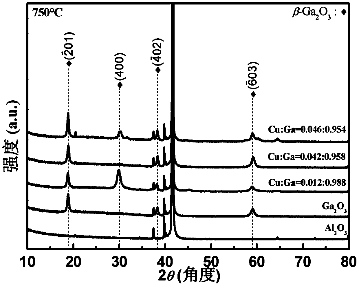
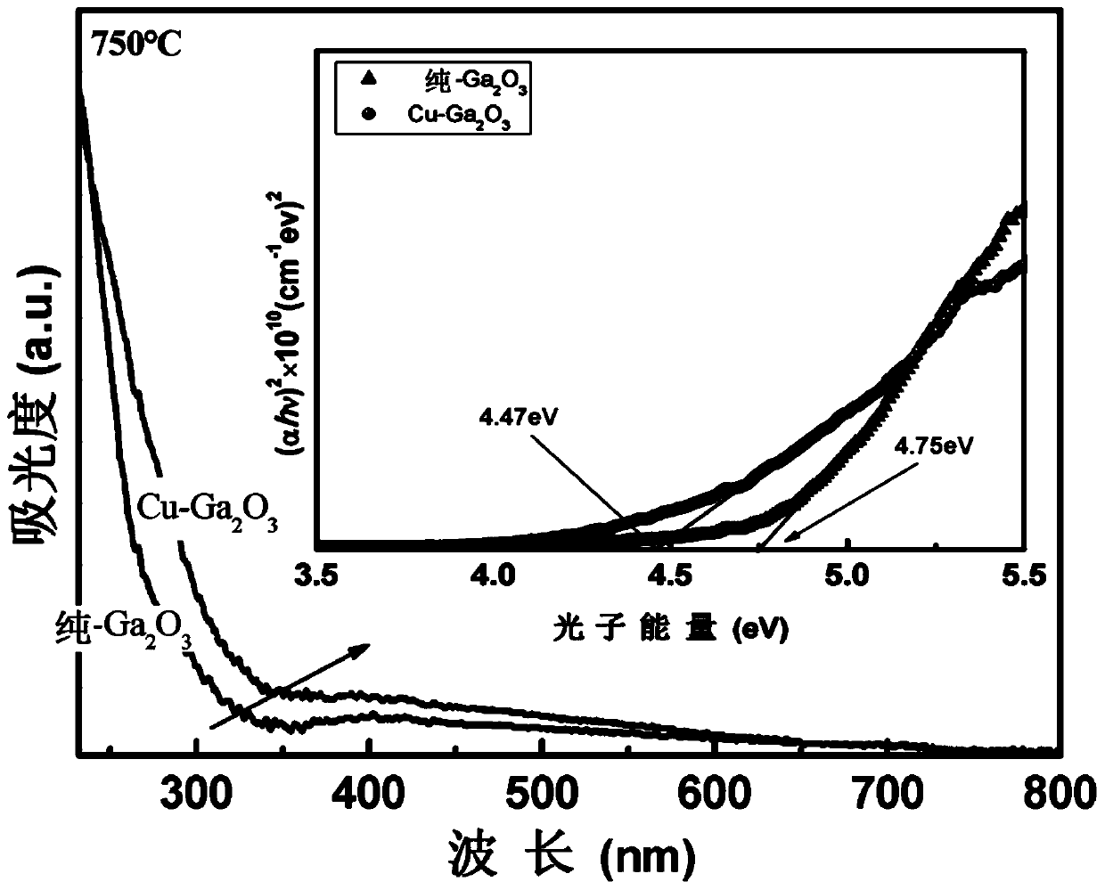
[0031] First take a piece of c-plane sapphire substrate and soak it in acetone, ethanol, and deionized water for 10 minutes, then rinse it with deionized water after taking it out, and finally wash it with dry N 2 Blow dry and set aside. Put the above-mentioned cleaned sapphire substrate into the deposition chamber, and grow a layer of Cu-doped Ga with a thickness of about 700 nm on it by magnetron sputtering 2 o 3 film. Ga in 99.99% purity 2 o 3 Ceramics are used as the main target, and pure Cu is used as the secondary target. Fixed Cu sputtering power 7W, Ga 2 o 3 The sputtering power was adjusted to 80W. The specific parameters of film growth are as follows: the background vacuum is 1×10 -4 Pa, the working atmosphere is Ar gas, the working pressure is 0.8Pa, the substrate temperature is 750°C, and the sputtering time is 5h. Ga 2 o 3 film at N 2 Medium annealing for 10h, the annealing temperature is 750°C. Cu:Ga=0.046:0.954 can be obtained by XPS analysis.
Embodiment 2
[0033] First take a piece of c-plane sapphire substrate and soak it in acetone, ethanol, and deionized water for 10 minutes, then rinse it with deionized water after taking it out, and finally wash it with dry N 2 Blow dry and set aside. Put the above-mentioned cleaned sapphire substrate into the deposition chamber, and grow a layer of Cu-doped Ga with a thickness of about 700 nm on it by magnetron sputtering 2 o 3 film. Ga in 99.99% purity 2 o 3 Ceramics are used as the main target, and pure Cu is used as the secondary target. Fixed Cu sputtering power 7W, Ga 2 o 3The sputtering power was adjusted to 100W. The specific parameters of film growth are as follows: the background vacuum is 1×10 -4 Pa, the working atmosphere is Ar gas, the working pressure is 0.8Pa, the substrate temperature is 750°C, and the sputtering time is 5h. Ga 2 o 3 film at N 2 Medium annealing for 10h, the annealing temperature is 750°C. Cu:Ga=0.031:0.969 can be obtained by XPS analysis.
Embodiment 3
[0035] First take a piece of c-plane sapphire substrate and soak it in acetone, ethanol, and deionized water for 10 minutes, then rinse it with deionized water after taking it out, and finally wash it with dry N 2 Blow dry and set aside. Put the above-mentioned cleaned sapphire substrate into the deposition chamber, and grow a layer of Cu-doped Ga with a thickness of about 700 nm on it by magnetron sputtering 2 o 3 film. Ga in 99.99% purity 2 o 3 Ceramics are used as the main target, and pure Cu is used as the secondary target. Fixed Cu sputtering power 7W, Ga 2 o 3 The sputtering power was adjusted to 120W. The specific parameters of film growth are as follows: the background vacuum is 1×10 -4 Pa, the working atmosphere is Ar gas, the working pressure is 0.8Pa, the substrate temperature is 750°C, and the sputtering time is 5h. Ga 2 o 3 film at N 2 Medium annealing for 10h, the annealing temperature is 750°C. Cu:Ga=0.012:0.988 can be obtained by XPS analysis.
PUM
| Property | Measurement | Unit |
|---|---|---|
| thickness | aaaaa | aaaaa |
| thickness | aaaaa | aaaaa |
Abstract
Description
Claims
Application Information
 - R&D
- Intellectual Property
- Life Sciences
- Materials
- Tech Scout
- Unparalleled Data Quality
- Higher Quality Content
- 60% Fewer Hallucinations
Browse by: Latest US Patents, China's latest patents, Technical Efficacy Thesaurus, Application Domain, Technology Topic, Popular Technical Reports.
© 2025 PatSnap. All rights reserved.Legal|Privacy policy|Modern Slavery Act Transparency Statement|Sitemap|About US| Contact US: help@patsnap.com


