
A kind of silicon-based molybdenum disulfide heterojunction photoelectric sensor and preparation method thereof

A silicon-based molybdenum disulfide, photoelectric sensor technology, applied in circuits, electrical components, semiconductor devices, etc., can solve the problems of low light absorption rate, high light response current, complex preparation process, etc., to improve light absorption efficiency and fast response. time, reducing the effect of compounding

Active Publication Date: 2020-12-29
UNIV OF ELECTRONICS SCI & TECH OF CHINA
View PDF7 Cites 0 Cited by
  • Summary
  • Abstract
  • Description
  • Claims
  • Application Information

AI Technical Summary

Problems solved by technology

However, MoS 2 The light absorption efficiency is determined by the number of layers, and the single-layer MoS 2 The light absorption rate is also low, resulting in a low photoresponse current; with the increase of the number of layers, the band gap further decreases while the light absorption rate increases, so the multilayer molybdenum disulfide with more than 10 layers has a lower High photoresponse current and can detect near-infrared light
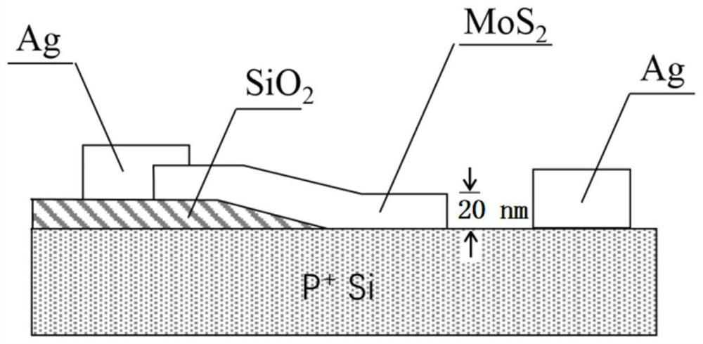
[0004] Da Ye Song et al. have reported a multilayer molybdenum disulfide / silicon heterojunction photodetector and its fabrication method. The device structure is as follows: figure 2 As shown; the preparation process of this structure is extremely complicated, and it is first necessary to etch SiO 2 layer as an insulating layer; secondly, it is required to accurately transfer small-sized molybdenum disulfide to Si and SiO 2 The edge of this operation is extremely difficult to control; at the same time, the electric field applied by the electrodes to the heterojunction region is a transverse electric field, which makes it difficult to achieve the effect of rapid separation of photogenerated carriers, making it difficult to improve the response time

Method used


Image

  • A kind of silicon-based molybdenum disulfide heterojunction photoelectric sensor and preparation method thereof
  • A kind of silicon-based molybdenum disulfide heterojunction photoelectric sensor and preparation method thereof
  • A kind of silicon-based molybdenum disulfide heterojunction photoelectric sensor and preparation method thereof

Examples


Embodiment 1

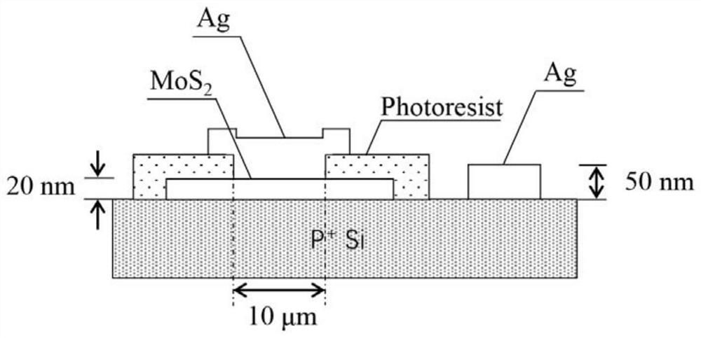
[0024] This example provides MoS based on multilayer thickness molybdenum disulfide 2 / Si heterojunction photosensor, its structure is as figure 1 As shown, including: P-type heavily doped silicon substrate, multi-layer molybdenum disulfide (MoS 2 ), photoresist (Photoresist), top electrode and bottom electrode; wherein, the multilayer molybdenum disulfide is arranged on the upper surface of the P-type heavily doped silicon substrate; the photoresist is coated on the multilayer molybdenum disulfide The upper surface is covered with multiple layers of molybdenum disulfide; a window is opened on the photoresist, and the top electrode is arranged on the multi-layer molybdenum disulfide through the window, and conducts with the multi-layer molybdenum disulfide; the bottom electrode It is arranged on the upper or lower surface of the P-type heavily doped silicon substrate.

[0025] In this embodiment, the number of layers of multilayer molybdenum disulfide is more than 10, the t...


PUM

PropertyMeasurementUnit
thicknessaaaaaaaaaa
heightaaaaaaaaaa

Abstract

The invention belongs to the field of photoelectric sensors, and provides a silicon-based molybdenum disulfide heterojunction photoelectric sensor and a preparation method thereof, which are used to overcome the disadvantages of complex preparation processes of existing multilayer molybdenum disulfide / silicon heterojunction photodetectors. In the present invention, the multi-layer molybdenum disulfide is directly arranged on the upper surface of the silicon substrate without precise transfer, and the photoresist is directly used as the insulating layer to effectively avoid SiO 2 layer, and the top electrode is directly arranged on the top of the multi-layer molybdenum dioxide by opening a window on the photoresist, which greatly reduces the difficulty of top electrode preparation, that is, the structure is simple and the preparation process is difficult; at the same time, the sensor of the present invention can be used in visible light It has a good photoelectric response in the near-infrared region, and the response time can reach 150-200us, that is, the sensitivity is higher.

Description

technical field [0001] The invention belongs to the field of photoelectric sensors, and relates to the preparation of a two-dimensional material heterojunction photoelectric sensor, in particular to a silicon-based molybdenum disulfide heterojunction photoelectric sensor and a preparation method thereof. Background technique [0002] With the rapid development of science and technology and the continuous progress of society, people have more and more demands for information; the integration technology of optoelectronic devices involves various fields such as military and national economy. Information systems play an increasingly important role in the evolution and development process. The band gap of transition metal sulfides changes with the number of layers, which makes them very suitable for applications in optoelectronic devices; among various transition metal sulfides, molybdenum disulfide (MoS 2 ) has been extensively studied as the most representative material. [0...

Claims


Application Information

Patent Timeline
Patent Type & Authority Patents(China)
IPC IPC(8): H01L31/109H01L31/0336H01L31/18C23C14/16C23C14/34
CPCY02P70/50
Inventor 黄文雷智程柯逸臻贺振北郭俊雄毛琳娜龚天巡
Owner UNIV OF ELECTRONICS SCI & TECH OF CHINA
Learn More