Magnesium-doped enhanced GaN-based HEMT device and preparation method thereof
An enhanced and device technology, applied in semiconductor/solid-state device manufacturing, semiconductor devices, electrical components, etc., can solve problems such as high cost, complicated process conditions, and long time, and achieve low cost, optimized device performance, and short time Effect
- Summary
- Abstract
- Description
- Claims
- Application Information
AI Technical Summary
Problems solved by technology
Method used
Image


Examples
Embodiment 1
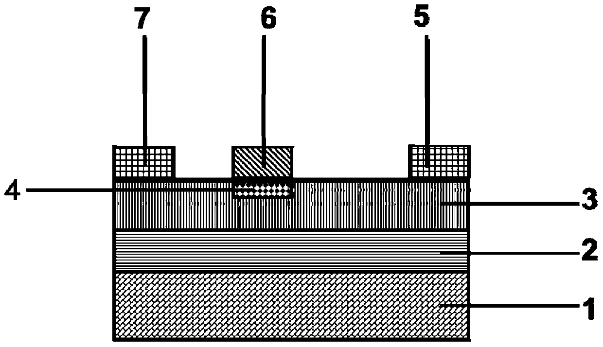
[0040] (1) Al on silicon-based GaN epitaxial wafers x Ga 1-x Photolithography on the N barrier layer prepares the gate electrode contact window to obtain a device containing the gate electrode contact window; the Al x Ga 1-x In the N barrier layer, the value of x is 0.01;
[0041] (2) On the surface of the contact window of the gate electrode in step (1), a layer of magnesium metal is deposited by electron beam evaporation, the thickness of the magnesium metal is 10nm; a device containing magnesium metal is obtained;
[0042] (3) performing stripping treatment on the unexposed photoresist on the magnesium-containing device described in step (2), to obtain the stripped device;
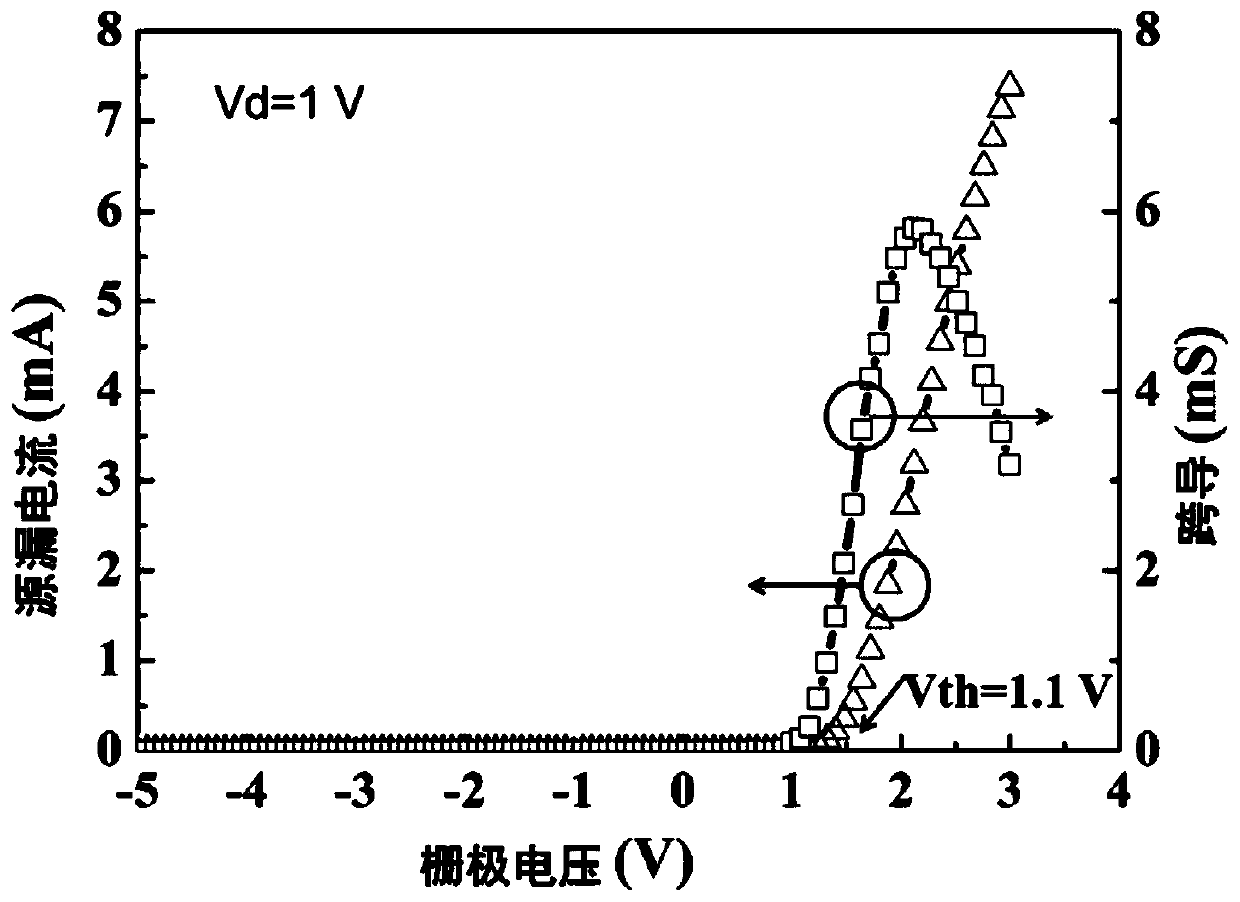
[0043] (4) Perform thermal annealing treatment on the device after the stripping treatment described in step (3) by using a thermal annealing process, so that the metal magnesium is diffused and doped into Al x Ga 1-x The N barrier layer forms a P-type AlGaN doped layer to obtain a device after the...
Embodiment 2
[0051] (1) Al on silicon-based GaN epitaxial wafers x Ga 1-x Photolithography on the N barrier layer prepares the gate electrode contact window to obtain a device containing the gate electrode contact window; the Al x Ga 1-x In the N barrier layer, the value of x is 0.25;
[0052] (2) Depositing a layer of metal magnesium on the surface of the gate electrode contact window in step (1) by means of electron beam evaporation, the thickness of the metal magnesium being 100 nm; obtaining a device containing metal magnesium;
[0053] (3) performing stripping treatment on the unexposed photoresist on the magnesium-containing device described in step (2), to obtain the stripped device;
[0054] (4) Perform thermal annealing treatment on the device after the stripping treatment described in step (3) by using a thermal annealing process, so that the metal magnesium is diffused and doped into Al x Ga 1-x The N barrier layer forms a P-type AlGaN doped layer to obtain a device after t...
Embodiment 3
[0060] (1) Al on silicon-based GaN epitaxial wafers x Ga 1-x Photolithography on the N barrier layer prepares the gate electrode contact window to obtain a device containing the gate electrode contact window; the Al x Ga 1-x In the N barrier layer, the value of x is 0.5;
[0061] (2) On the surface of the contact window of the gate electrode in step (1), a layer of magnesium metal is deposited by electron beam evaporation, the thickness of the magnesium metal is 200nm; a device containing magnesium metal is obtained;
[0062] (3) performing stripping treatment on the unexposed photoresist on the magnesium-containing device described in step (2), to obtain the stripped device;
[0063] (4) Perform thermal annealing treatment on the device after the stripping treatment described in step (3) by using a thermal annealing process, so that the metal magnesium is diffused and doped into Al x Ga 1-x The N barrier layer forms a P-type AlGaN doped layer to obtain a device after the...
PUM
| Property | Measurement | Unit |
|---|---|---|
| thickness | aaaaa | aaaaa |
| thickness | aaaaa | aaaaa |
| thickness | aaaaa | aaaaa |
Abstract
Description
Claims
Application Information
 - Generate Ideas
- Intellectual Property
- Life Sciences
- Materials
- Tech Scout
- Unparalleled Data Quality
- Higher Quality Content
- 60% Fewer Hallucinations
Browse by: Latest US Patents, China's latest patents, Technical Efficacy Thesaurus, Application Domain, Technology Topic, Popular Technical Reports.
© 2025 PatSnap. All rights reserved.Legal|Privacy policy|Modern Slavery Act Transparency Statement|Sitemap|About US| Contact US: help@patsnap.com