Laminated silicon-doped tin oxide thin film transistor and preparation method thereof
A technology of thin film transistors and silicon doping, applied in the direction of transistors, semiconductor/solid-state device manufacturing, semiconductor devices, etc., can solve the problems of unstable optical bias voltage and low mobility, achieve low annealing temperature, simple preparation process, good The effect of device performance
- Summary
- Abstract
- Description
- Claims
- Application Information
AI Technical Summary
Problems solved by technology
Method used
Image

Examples
Embodiment 1
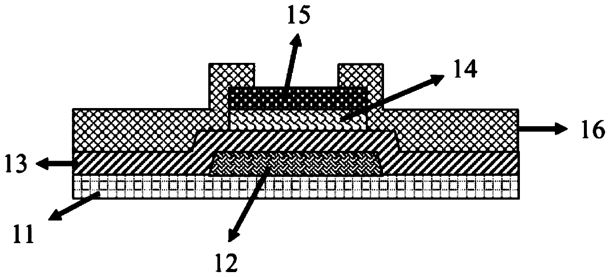
[0038] A stacked silicon-doped tin oxide thin film transistor in this embodiment includes a substrate, a gate, a gate insulating layer, a first active layer, a second active layer, and source and drain electrodes stacked in sequence. Its layered structure diagram is shown in figure 1 shown. Its preparation method is as follows:
[0039] (1) At room temperature, an aluminum gate is prepared on a glass substrate by DC magnetron sputtering and patterned;
[0040] (2) On the gate, an aluminum oxide gate insulating layer is grown by an anodic oxidation method;
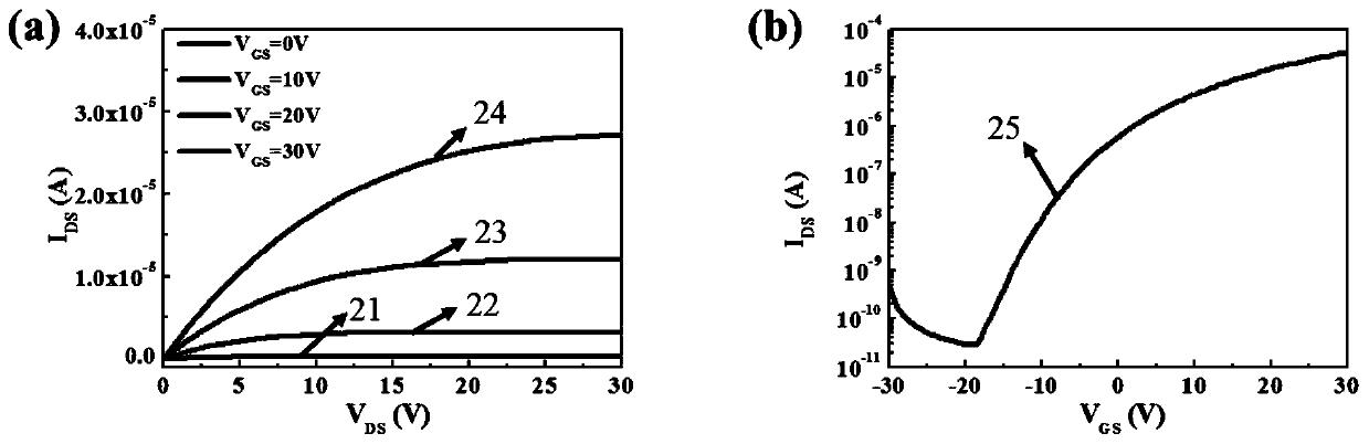
[0041] (3) On the gate insulating layer, utilize a mask plate to deposit a first layer of active layer with a thickness of 5 nm by radio frequency magnetron sputtering; the material of the first layer of active layer is 3% by mass of silicon Silicon-doped tin oxide;
[0042] (4) Annealing the prepared sample at 250°C on a hot stage;
[0043] (5) Utilize the same mask plate as step (3), on the first active layer, deposi...
Embodiment 2
[0047] A stacked silicon-doped tin oxide thin film transistor in this embodiment includes a substrate, a gate, a gate insulating layer, a first active layer, a second active layer, and source and drain electrodes stacked in sequence. Its layered structure diagram is shown in figure 1 shown. Its preparation method is as follows:
[0048] (1) At room temperature, an aluminum gate is prepared on a glass substrate by DC magnetron sputtering and patterned;
[0049] (2) On the gate, an aluminum oxide gate insulating layer is grown by an anodic oxidation method;
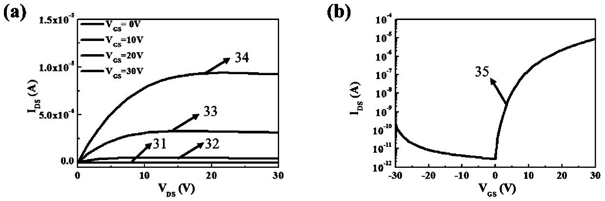
[0050] (3) On the gate insulating layer, utilize a mask plate to deposit a first layer of active layer with a thickness of 5 nm by radio frequency magnetron sputtering; the material of the first layer of active layer is 0% by mass of silicon tin oxide;
[0051] (4) Annealing the prepared sample at 250°C on a hot stage;
[0052] (5) Utilize the same mask plate as step (3), on the first active layer, deposit the second a...
Embodiment 3
[0056] A stacked silicon-doped tin oxide thin film transistor in this embodiment includes a substrate, a gate, a gate insulating layer, a first active layer, a second active layer, and source and drain electrodes stacked in sequence. Its layered structure diagram is shown in figure 1 shown. Its preparation method is as follows:
[0057] (1) At room temperature, an aluminum gate is prepared on a glass substrate by DC magnetron sputtering and patterned;
[0058] (2) On the gate, an aluminum oxide gate insulating layer is grown by an anodic oxidation method;
[0059] (3) On the gate insulating layer, utilize a mask plate to deposit a first layer of active layer with a thickness of 5 nm by radio frequency magnetron sputtering; the material of the first layer of active layer is 1% by mass of silicon Silicon-doped tin oxide;
[0060] (4) Annealing the prepared sample at 250°C on a hot stage;
[0061] (5) Utilize the same mask plate as step (3), on the first active layer, deposi...
PUM
 Abstract
Description
Claims
Application Information
 - Generate Ideas
- Intellectual Property
- Life Sciences
- Materials
- Tech Scout
- Unparalleled Data Quality
- Higher Quality Content
- 60% Fewer Hallucinations
Browse by: Latest US Patents, China's latest patents, Technical Efficacy Thesaurus, Application Domain, Technology Topic, Popular Technical Reports.
© 2025 PatSnap. All rights reserved.Legal|Privacy policy|Modern Slavery Act Transparency Statement|Sitemap|About US| Contact US: help@patsnap.com